Variable impedance load for a variable gain radio frequency amplifier

a radio frequency amplifier and variable gain technology, applied in amplifiers, amplifiers with semiconductor devices/discharge tubes, electrical devices, etc., can solve the problems of reducing the flatness of the filter gain, reducing the in-band and out-of-band characteristics of the transmit filter, and increasing the loss of the insertion of the filter

Inactive Publication Date: 2006-09-26
QUALCOMM INC
View PDF11 Cites 26 Cited by
  • Summary
  • Abstract
  • Description
  • Claims
  • Application Information

AI Technical Summary

Benefits of technology

[0016]The variable impedance load may comprise a transistor in series with a resistor wherein the transistor is controlled by a c...

Problems solved by technology

The impedance mismatch also adversely affects the operation of the transmit filter 14 resulting in a degradation of the in-band and out-of-band characteris...

Method used


Image

  • Variable impedance load for a variable gain radio frequency amplifier
  • Variable impedance load for a variable gain radio frequency amplifier
  • Variable impedance load for a variable gain radio frequency amplifier

Examples


Embodiment Construction

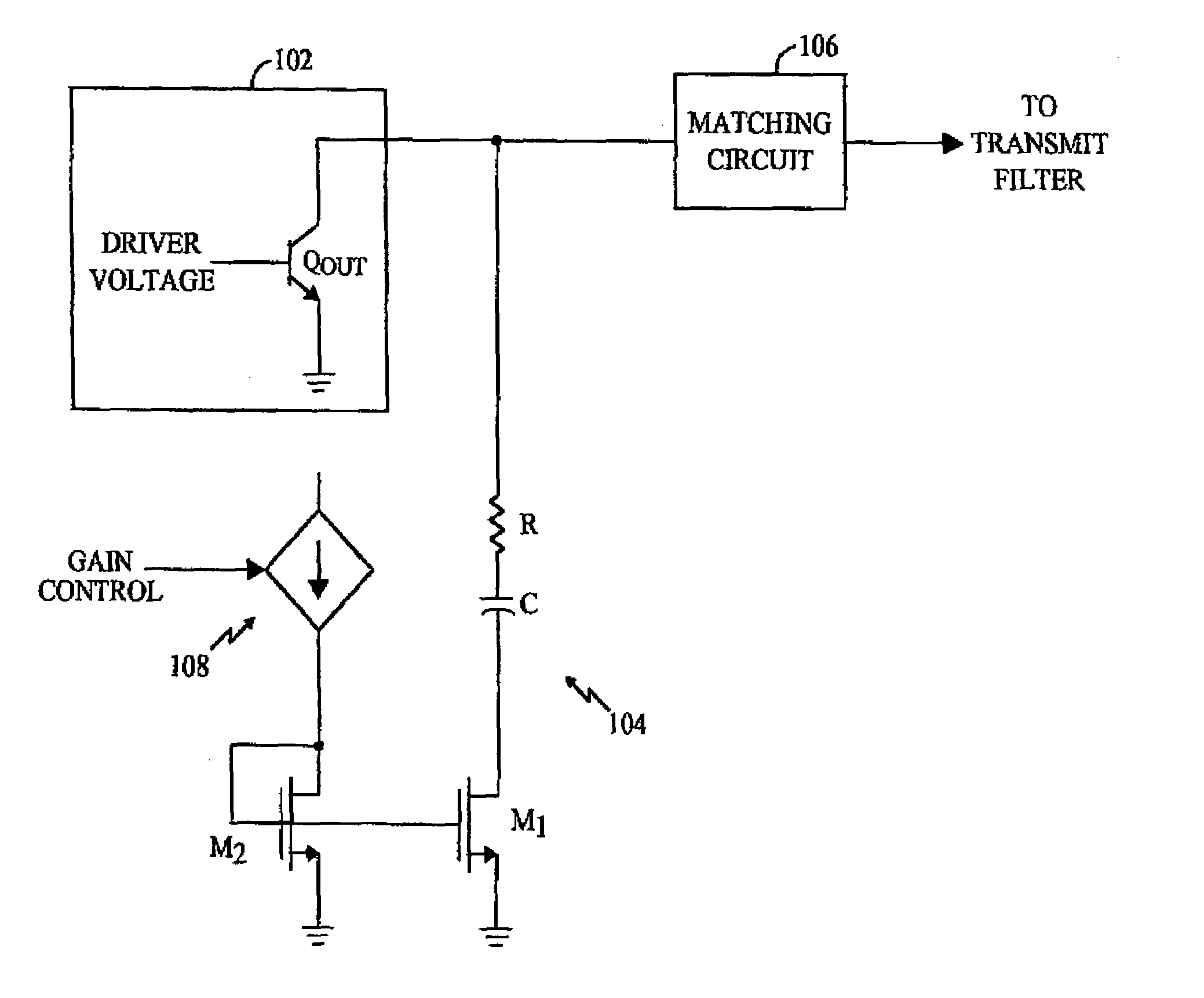
[0024]The present invention provides a variable impedance load whose input impedance varies based on the gain of a variable gain RF driver amplifier.

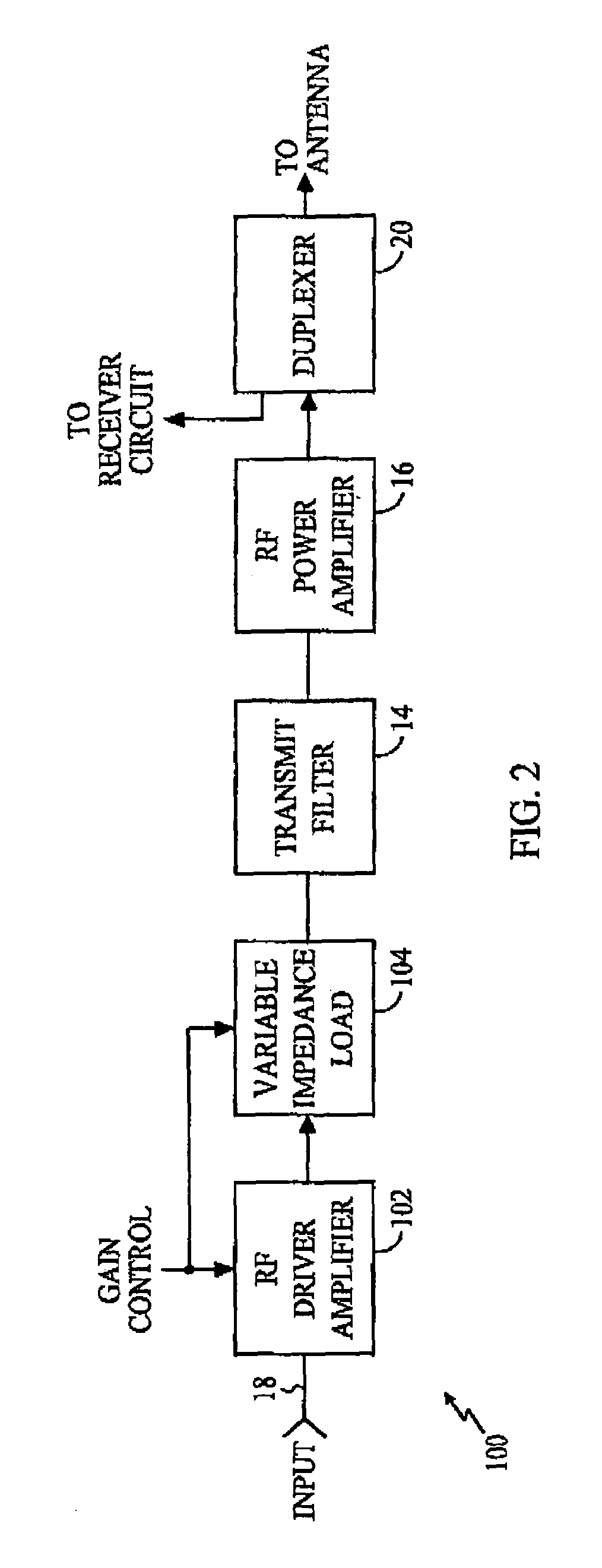
[0025]An exemplary embodiment of the present invention is illustrated in a system 100, illustrated as a functional block diagram in FIG. 2. An RF driver amplifier 102 has a gain control input. In an exemplary embodiment, the RF driver amplifier 102 has a variable gain of approximately 20–40 decibels (dB). As those skilled in the art will appreciate, the output impedance of the RF driver amplifier 102 varies significantly as a function of the gain of the amplifier. Specifically, as the gain of the amplifier increases, the output current of the RF driver amplifier 102 increases and the output impedance decreases. Conversely, as the gain of the RF driver amplifier 102 decreases, the output current decreases and the output impedance of the RF driver amplifier increases. Thus, the output impedance varies inversely with the gain (and the outp...


PUM


Abstract

A variable impedance load (104) is provided at the output of a radio frequency (RF) driver amplifier (102) having a variable gain. In an exemplary embodiment, the variable load (104) comprises a resistor (R) in series with a semiconductor device (M1). The semiconductor device (M1) has an impedance level determined by a drive current. The value of the drive current is related to the gain of the RF driver amplifier (102).

Description

BACKGROUND OF THE INVENTION[0001]1. Field of the Invention[0002]The present invention is directed generally to wireless communication devices and, more particularly, to a variable impedance load for a variable gain radio frequency amplifier used in the output stage of a wireless communication device.[0003]2. Description of the Related Art[0004]The use of wireless communication devices, in applications such as wireless telephones, is widespread. The output stage of a wireless communication device includes radio frequency (RF) amplifiers. This is true of most wireless communication devices regardless of the form of modulation, such as AM, FM, and the like. A typical output stage 10 for a wireless communication device is illustrated in FIG. 1 and comprises an RF driver amplifier 12, a transmit filter 14, and an RF power amplifier 16. An output port of the RF driver amplifier 12 is coupled to an input port of the transmit filter 14. Similarly, an output port of the transmit filter 14 is...

Claims


Application Information

Patent Timeline
IPC IPC(8): H03G3/20H03G3/30H03H11/30
CPCH03H11/30H03G3/3042
Inventor BARNETT, KENNETH
Owner QUALCOMM INC
Why Eureka
Try Eureka