Probe for scanning probe lithography and making method thereof
a scanning probe and lithography technology, applied in the direction of microstructural devices, material analysis using wave/particle radiation, nuclear engineering, etc., can solve the problems of affecting the use of the probe, the tip of the probe is likely to be deformed, and the lithography is not suitable for scanning. to achieve the effect of increasing the mechanical strength of the conductor
- Summary
- Abstract
- Description
- Claims
- Application Information
AI Technical Summary
Benefits of technology
Problems solved by technology
Method used
Image

Examples
embodiment i
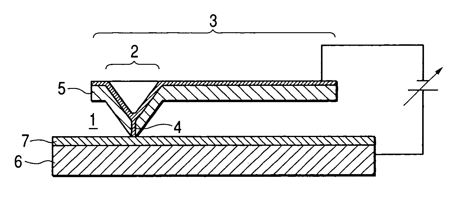
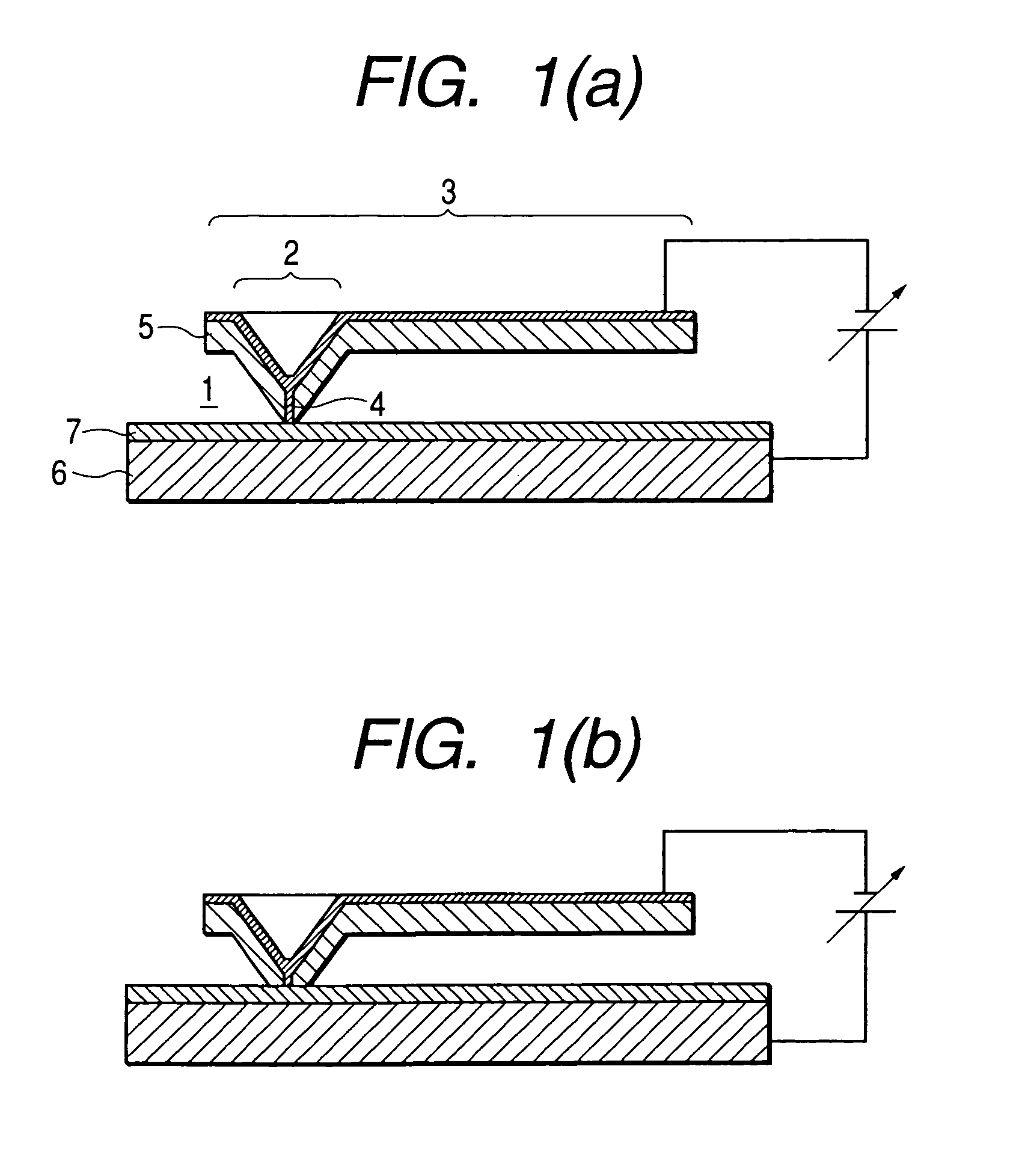
[0030]In the present preferred embodiment, a lithographic scanning probe comprises a spring section and a tip part in a structure similar to a conventional probe for atomic force microscopy, and the spring section is structured in a micro-cantilever form. Arranged as mentioned above, the lithographic scanning probe is applicable to scanning probe lithography systems such as those proposed in Journal of Vacuum Science Technology B15 (1997), pp. 1811–1817, reported by K. Wilder et al., Japan Journal of Applied Physics 37 (1998), pp. 1565–1569, reported by M. Ishibashi et al., and Japanese Unexamined Patent Publication No. 11 (1999)-73906.
[0031]As to fabrication of a micro-cantilever type of probe for atomic force microscopy, there are known a micro-casting method, reported by T. R. Albrecht et al. in Journal of Vacuum Science Technology A8 (1990), pp. 3386–3396), an isotropic reactive ion etching method, a lift-off—evaporation combination method, etc. In the present preferred embodime...
embodiment ii
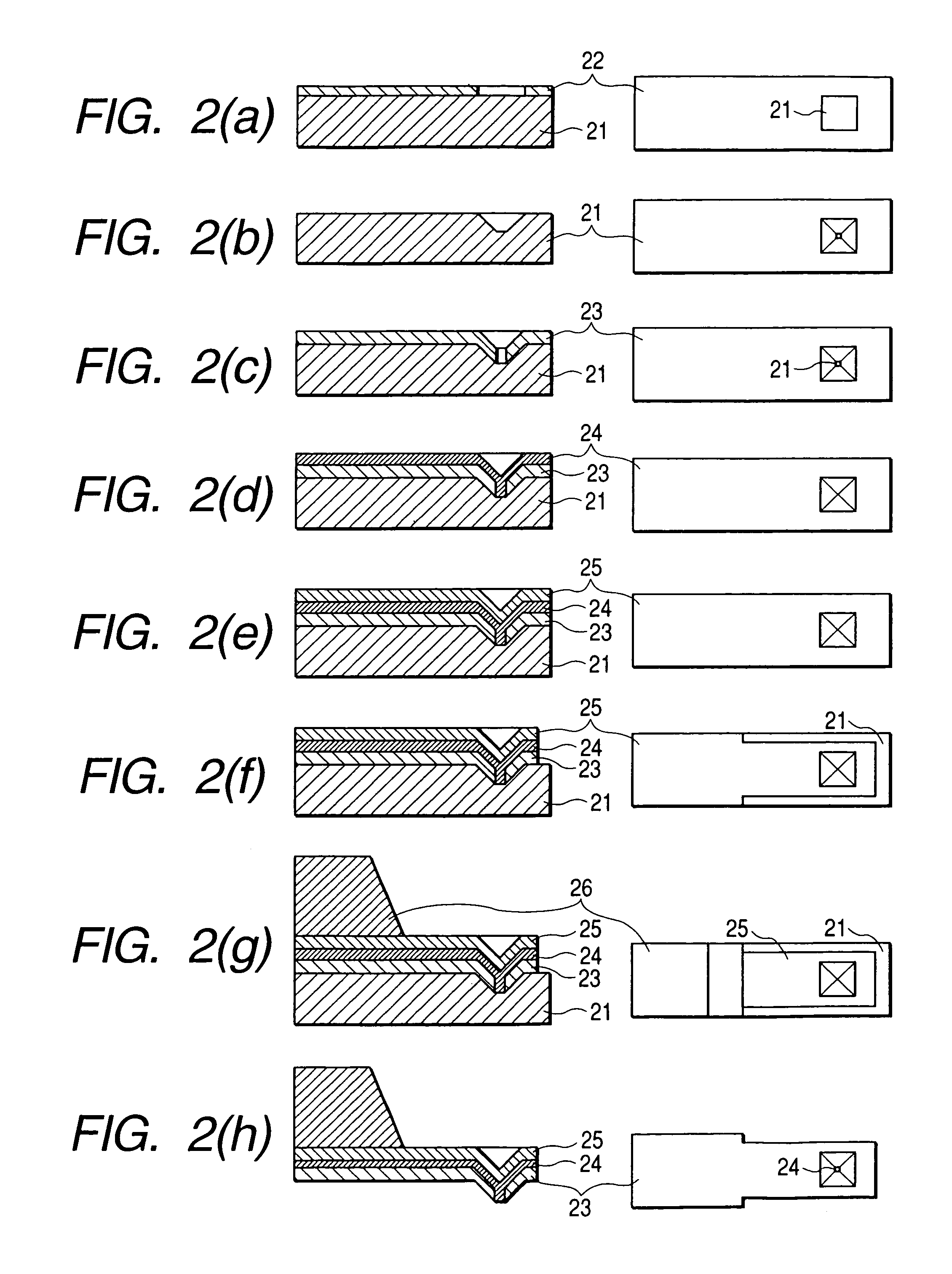
[0043]While the tip part having a quadrangular pyramid shape with a flat apex is formed in the preferred embodiment described above in connection with FIGS. 2(a) to 2(h), it is also preferable to form a tip part having a hemispherical shape. Referring to FIGS. 4(a) and 4(b), there are shown a spring section and a tip part formed in a hemispherical shape having a diameter of 4000 nm in another preferred embodiment of a lithographic scanning probe. FIG. 4(a) is a plan view of the lithographic scanning probe according to the present preferred embodiment as seen from a surface to be patterned, and FIG. 4(b) is a sectional view taken on line A—A of FIG. 4(a). For fabricating the hemispherical tip part shown in FIG. 4, a hemispherical hole therefor is formed on the silicon substrate 21. Instead of anisotropic etching with an aqueous solution of potassium hydroxide employed for forming the inverted quadrangular pyramid hole in the EMBODIMENT I, isotropic etching with a mixture solution of ...
embodiment iii
[0044]In the present preferred embodiment, there is provided a lithographic scanning probe in which a tip part thereof has a structure different from that in the EMBODIMENT I. The following describes the EMBODIMENT III with particular reference to FIGS. 5(a) to 5(c). In the EMBODIMENT III, the lithographic scanning probe has a three-layer structure comprising a conductive layer, an insulating layer and a vending-correction layer as in the EMBODIMENT I. A holder and a spring section of the lithographic scanning probe in the EMBODIMENT III are structured in the same fashion as in the EMBODIMENT I.
[0045]FIG. 5(a) shows a schematic diagram of the tip part in the EMBODIMENT III, as seen from a surface to be patterned, FIG. 5(b) is a sectional view taken on line A—A of FIG. 5(a) in the arrow direction, and FIG. 5(c) is a sectional view taken on line B—B of FIG. 5(a) in the arrow direction.
[0046]In the present preferred embodiment, it is assumed that the lithographic scanning probe moves i...
PUM
| Property | Measurement | Unit |
|---|---|---|
| Time | aaaaa | aaaaa |
| Thickness | aaaaa | aaaaa |
| Diameter | aaaaa | aaaaa |
Abstract
Description
Claims
Application Information