Solid-state semiconductor light emitting device

a light-emitting device and semiconductor technology, applied in semiconductor devices, semiconductor/solid-state device details, lighting and heating apparatus, etc., can solve the problems of easy damage to the packaging die and complicated composition, and achieve good heat-dissipating effect, enhance connection stability, and increase heat-dissipating area

Active Publication Date: 2006-10-10
EPISTAR CORP
View PDF5 Cites 126 Cited by
  • Summary
  • Abstract
  • Description
  • Claims
  • Application Information

AI Technical Summary

Benefits of technology

[0006]Another purpose of the present invention is to provide a solid-state semiconductor light emitting device that increases heat-dissipating area and enhances connection stability.
[0007]In order to achieve the aforementioned purposes, the present invention comprises a heat sink, a chip, a leadframe, and a resin or silicone that covers all of them, wherein a receiving cup is mounted on the center portion of the heat sink for receiving the chip. In addition, the chip is connected to the heat sink via a heat-conducting bracket. In the leadframe, two holders that include two top sides on their two top portions are opposite to one another, and a holder that includes holes on a center portion thereof is mounted between these two top sides. The holder having the holes on the center portion thereof is connected to one of these two opposite holders in a random position. These three holders are connected to one another by using a plastic material. The connection base is formed by molding the plastic material. The receiving cup of the heat sink is received by the connection base of the leadframe and the chip is connected to the leadframe via a metal wire. Next, the resin or silicone covers all of them so as to complete a light emitting diode that emits light. As a result, the heat sink provides with good heat-dissipating efficacy and each holder of the leadframe also provides with heat-dissipating efficacy and enhances the connection stability as well.

Problems solved by technology

Accordingly, the packaged die will be damaged easily as a result of thermal stress.
Although the above structure can separate electricity and heat from one another to prevent the die from heat, its composition is very complicated.

Method used


Image

  • Solid-state semiconductor light emitting device
  • Solid-state semiconductor light emitting device
  • Solid-state semiconductor light emitting device

Examples


Embodiment Construction

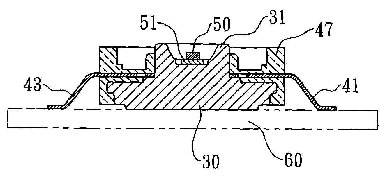
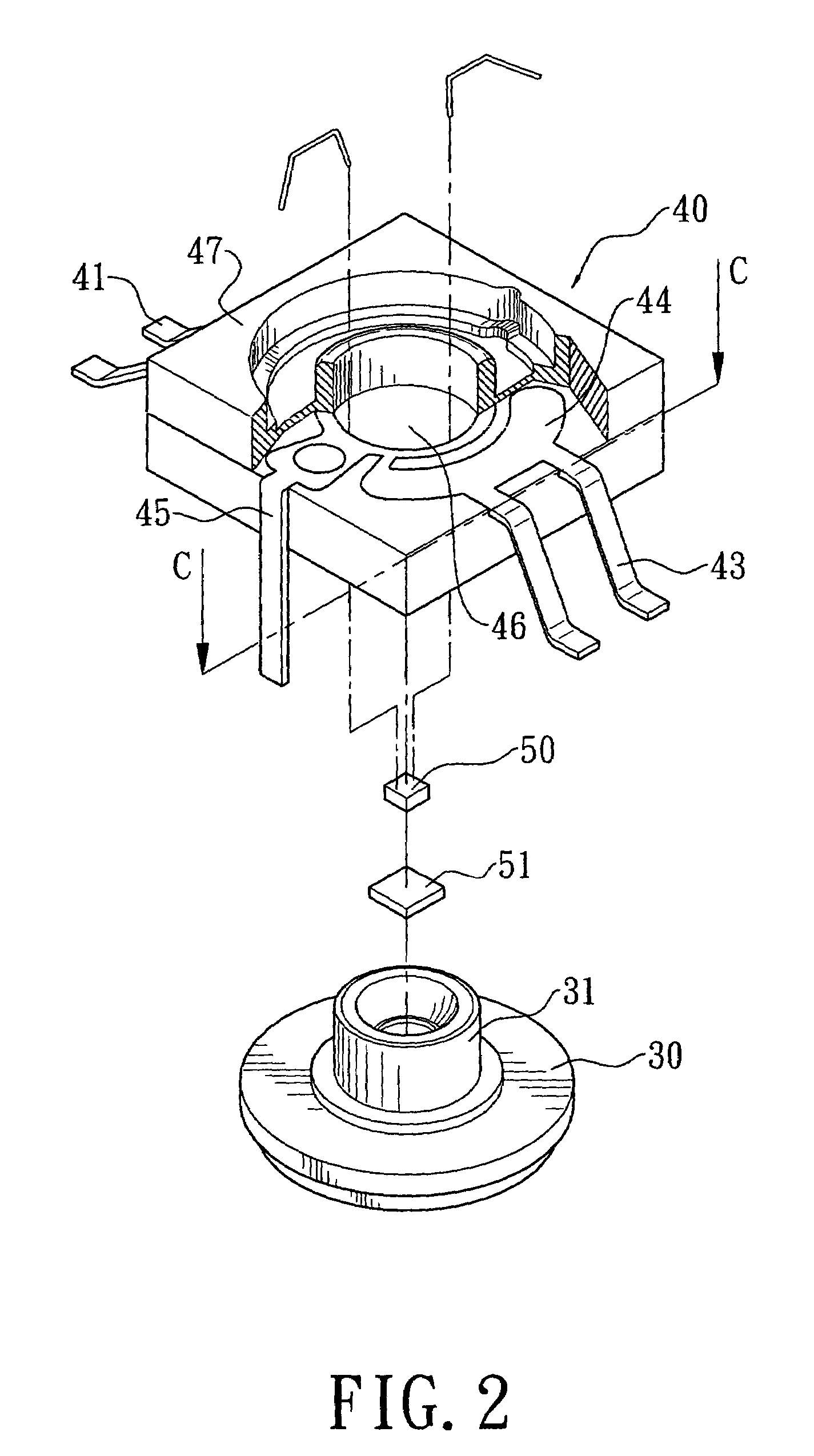
[0018]Referring to FIG. 1 and FIG. 2, the present invention mainly comprises a heat sink 30, a leadframe 40, a chip 50, and a heat-conducting bracket 51. Next, all of them are covered by resin or silicone (not shown) to form a light emitting diode. The heat sink 30 is made of a heat-conducting material selected from the group consisting of pure materials, compounds, and composites of copper, silicon, aluminum, molybdenum, aluminum oxide, aluminum nitride, and beryllium. Alternatively, composites of molybdenum-copper and tungsten-copper may be used. Receiving cup 31 projects upwardly from the center portion of the heat sink 30 for receiving the optional heat-conducting bracket 51 and the chip 50.

[0019]The leadframe 40 is formed by arranging a first holder 41, a second holder 43, and a third holder 45, and coupling them with a connection base 47, which is made of a molded plastic material. As shown in FIG. 6, the first holder 41 and the second holder 43 are identical in structure, whe...


PUM


Abstract

A solid-state semiconductor light emitting device is disclosed. A heat sink that comprises a receiving cup for receiving a chip is provided. A leadframe that comprises a connection base is mounted above the heat sink, wherein the chip is connected to the leadframe via a metal wire and a resin or silicone is applied to cover all of them so as to form the a light emitting device that emits light. In the leadframe, two holders that include two top sides on their two top portions are opposite to one another, and a holder having holes is mounted between these two top sides. The holder having the holes is connected to one of these two opposite holders. A plastic material is applied to mold the three holders into the connection base for receiving the receiving cup of the heat sink. As a result, the heat sink provides with good heat-dissipating efficacy and each holder of the leadframe also provides with heat-dissipating efficacy and enhances connection stability as well.

Description

FIELD OF THE INVENTION[0001]The present invention relates to a solid-state semiconductor light emitting device that provides with good heat-dissipating efficacy and enhances connection stability, and more particularly, to a solid-state semiconductor light emitting device that is suitable for a light emitting diode (LED) or the like.BACKGROUND OF THE INVENTION[0002]In general, photometric efficiency of an LED is inversely proportional to the junction temperature of the LED. A major concern of the LED package designer is keeping the die cool to be lower than the junction temperature. In the conventional LED, the chip is mounted at the base of a concave cup (i.e. optical cavity) of one conducting wire and connected to another conducting wire via a connection wire. Accordingly, the packaged die will be damaged easily as a result of thermal stress.[0003]In view of above conventional drawbacks, U.S. Pat. No. 6,274,924 entitled “surface mountable led package” discloses a structure, as show...

Claims


Application Information

Patent Timeline
Patent Type & Authority Patents(United States)
IPC IPC(8): H01L23/34
CPCH01L33/62H01L33/642H01L33/647H01L2924/0002H01L2924/00
Inventor CHIN, YUAN-CHENG
Owner EPISTAR CORP
Why Eureka
Try Eureka