

System and method for a data-input array capable of being scanned using a reduced number of signals
- Summary
- Abstract
- Description
- Claims
- Application Information
AI Technical Summary
Benefits of technology
Problems solved by technology
Method used
Image

Examples
Embodiment Construction
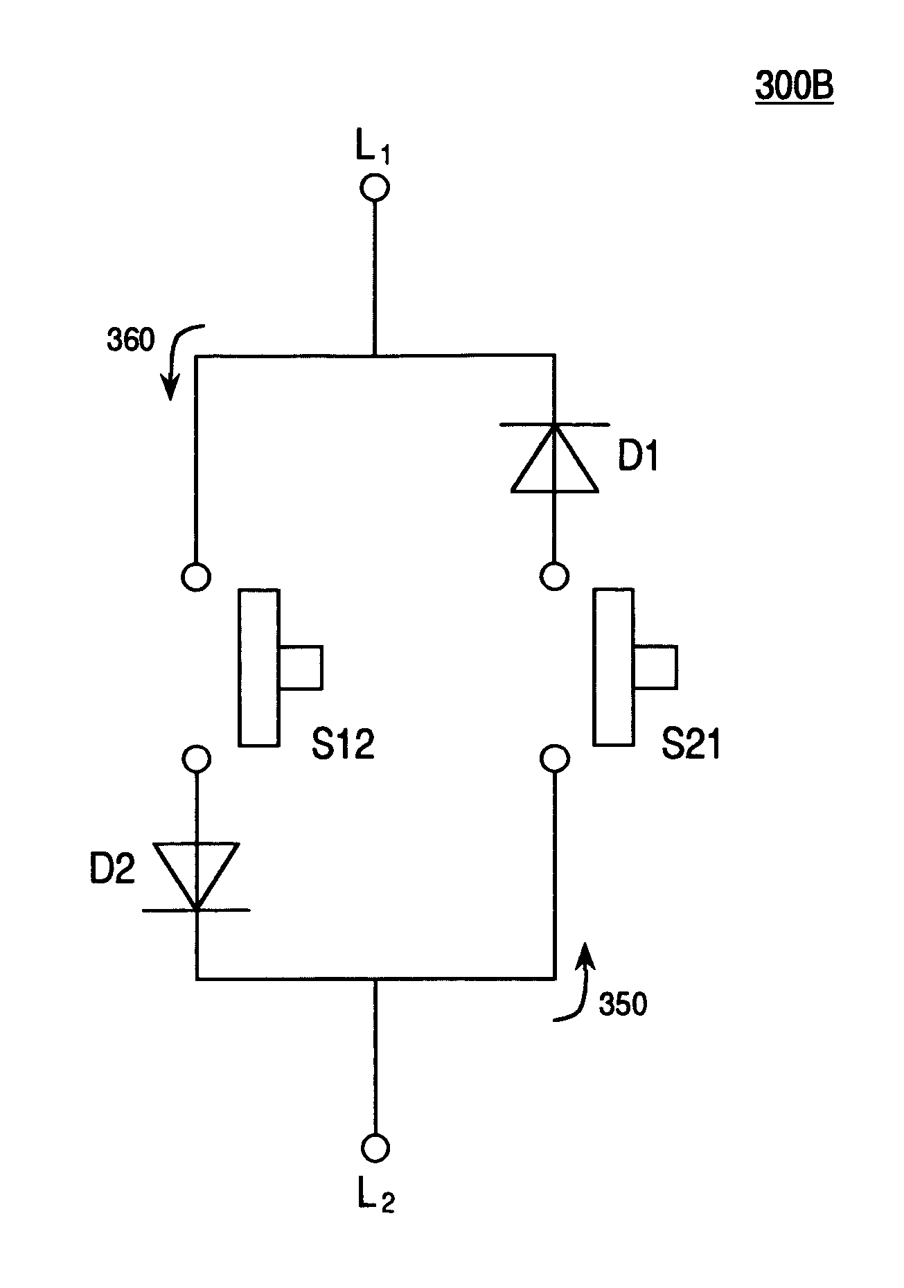
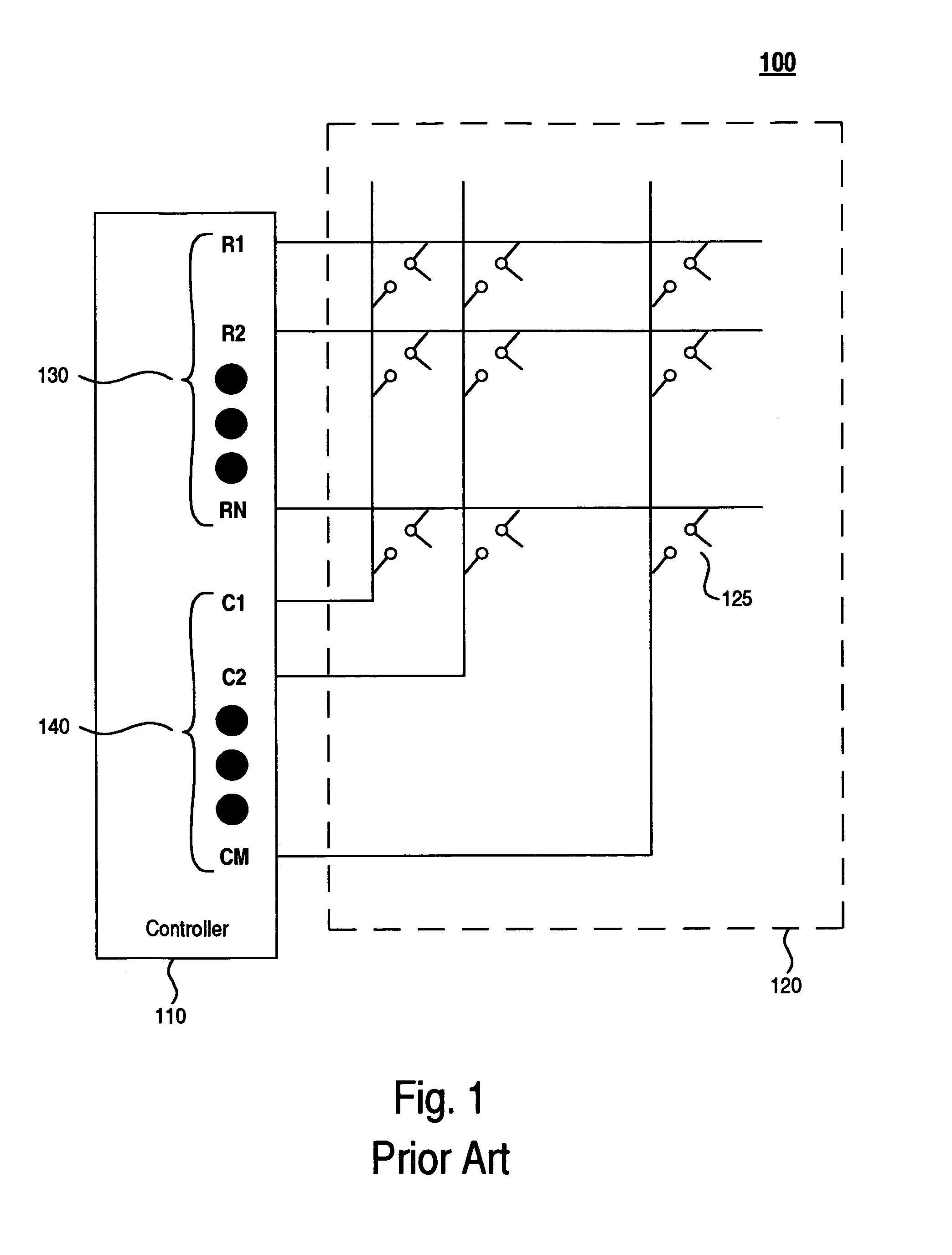
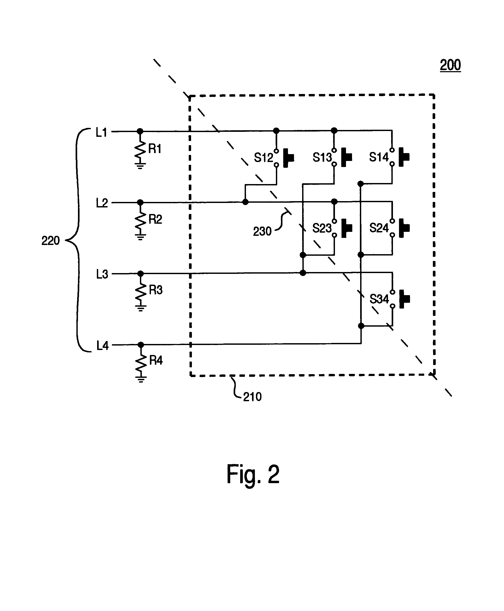
[0027]Reference will now be made in detail to the preferred embodiments of the present invention, a system and method for a switch array that is capable of being scanned using a reduced number of signals, examples of which are illustrated in the accompanying drawings.
[0028]Accordingly, various embodiments of the present invention disclose a system and method for a switch array that can be scanned using a reduced number of signals. As an advantage over the prior art, the present invention is capable of reducing the number of pins on a system controller used to scan a key matrix, to reduce manufacturing costs. As a further advantage, the present invention is capable of reducing the number of wires used to transmit signals between a system controller and a key matrix, thereby reducing the size and cost of cabling and ultimately reducing the manufacturing costs. Moreover, the present invention is capable of increasing the functionality and number of services provided by an integrated ci...
PUM
 Abstract
Description
Claims
Application Information