Apparatus and method for reducing stray light in substrate processing chambers

a technology of substrate processing chamber and apparatus, which is applied in the field of thermoplastic processing chamber, can solve the problems of limiting system design, unreasonably deviating from the actual or true non-uniform temperature of the substrate,

Inactive Publication Date: 2006-11-14
MATTSON TECHNOLOGY +1
View PDF84 Cites 32 Cited by
  • Summary
  • Abstract
  • Description
  • Claims
  • Application Information

AI Technical Summary

Benefits of technology

[0037]The present invention provides various benefits and advantages in determining the temperature of wafers during heating processes. In particular, the spectral filter can absorb and eliminate unwanted radiation from being sensed by the radiation sensing device for more accurately determining the temperature of the wafers. Of particular advantage, in one embodiment, a spectral filter made in accordance with the present invention can be chosen that is very efficient at absorbing light at relatively short wavelengths, such as wavelengths less than about 2 microns, and particularly at wavelengths less than about 1 micron. In other embodiments, however, spectral filters made in accordance with the present invention can be designed to absorb light at wavelengths longer than 2 microns which may be desired in some applications.

Problems solved by technology

One major problem in the design of rapid thermal processing chambers having an optical temperature measurement system, however, has been the ability to prevent unwanted light radiated by the heater lamps from being detected by the pyrometric instrumentation.
Should unwanted light not being emitted by the semiconductor wafer be detected by the pyrometer, the calculated temperature of the wafer may unreasonably deviate from the actual or true temperature of the wafer.
Physical barriers, however, can restrict the system design.
When a support ring is present, there can be overlap between the support ring and the edges of the wafer, which can lead to temperature non-uniformities in the wafer during heating cycles.
Another problem can arise if the support ring or the wafer is warped even slightly.
The stray light can induce errors in the pyrometer readings.
Silica glass, however, is unfortunately not well suited to being used as a spectral filter in temperature measurement systems that contain pyrometers that sense thermal radiation at shorter wavelengths, such as less than about one micron.
In the past, however, pyrometers that operate at lower wavelengths have been selectively used in thermal processing chambers due to the significant amount of stray light that can be detected in thermal processing chambers at lower wavelengths.

Method used


Image

  • Apparatus and method for reducing stray light in substrate processing chambers
  • Apparatus and method for reducing stray light in substrate processing chambers
  • Apparatus and method for reducing stray light in substrate processing chambers

Examples


Embodiment Construction

[0031]It is to be understood by one of ordinary skill in the art that the present discussion is a description of exemplary embodiments only, and is not intended as limiting the broader aspects of the present invention which broader aspects are embodied in the exemplary construction.

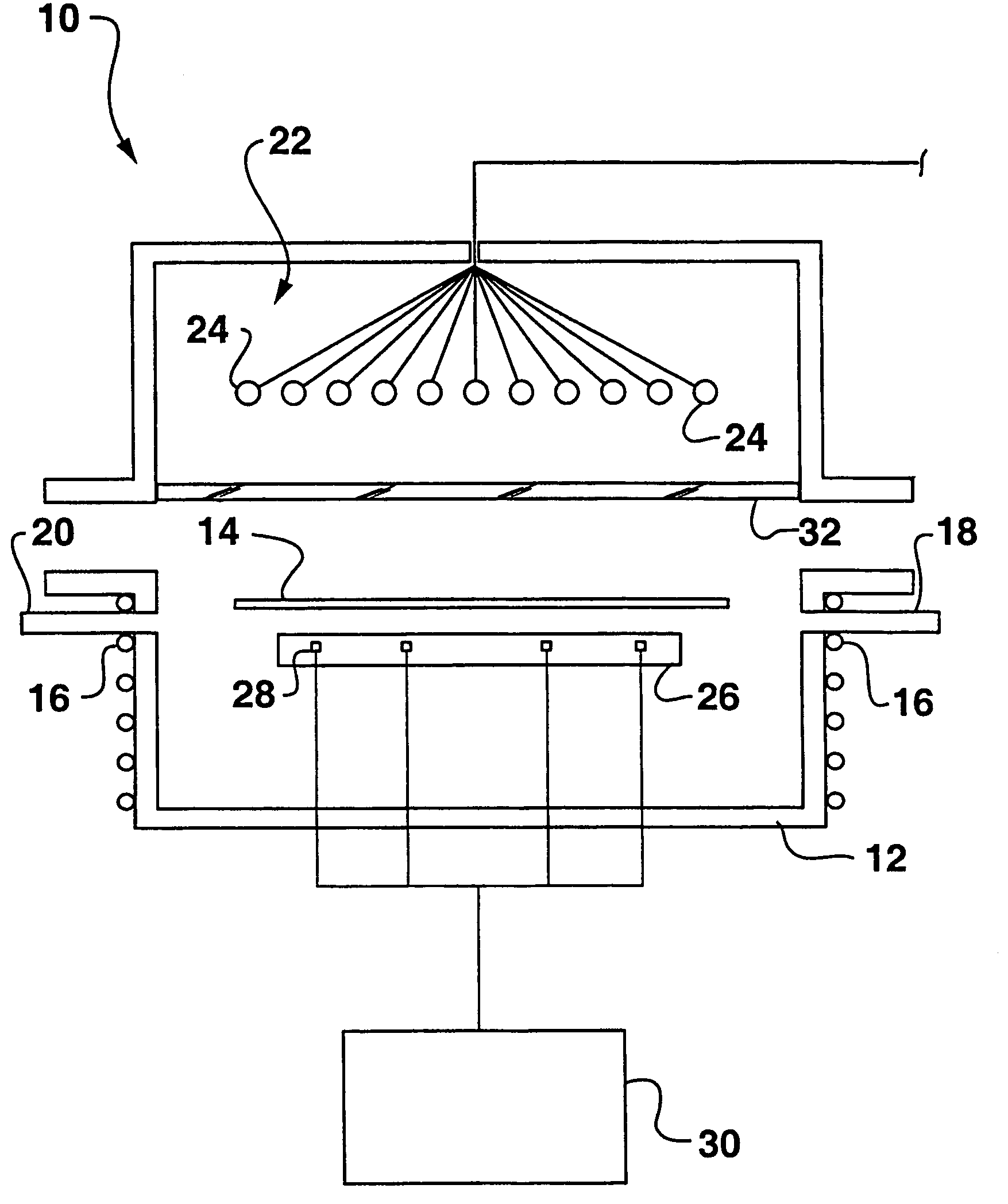
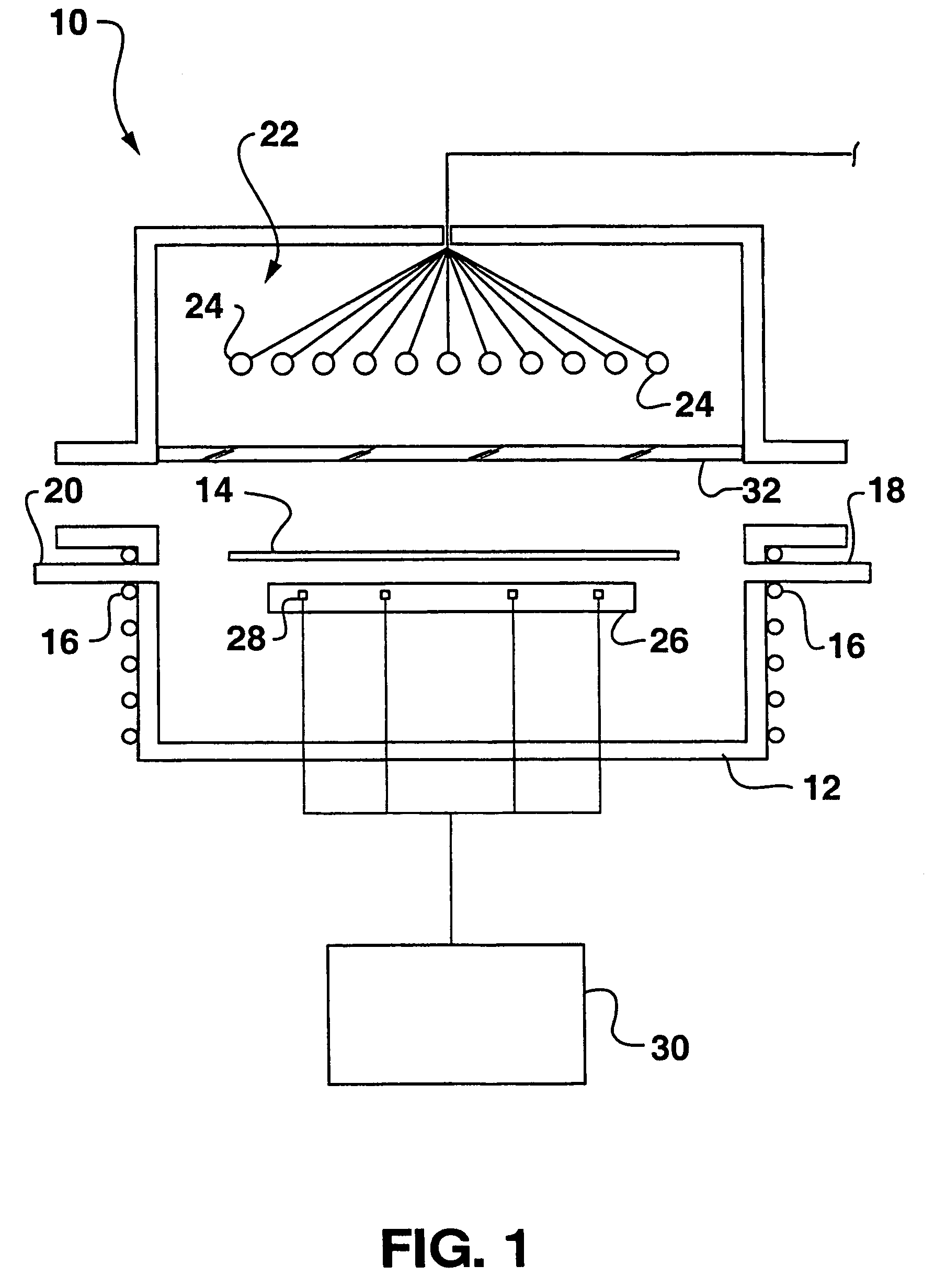
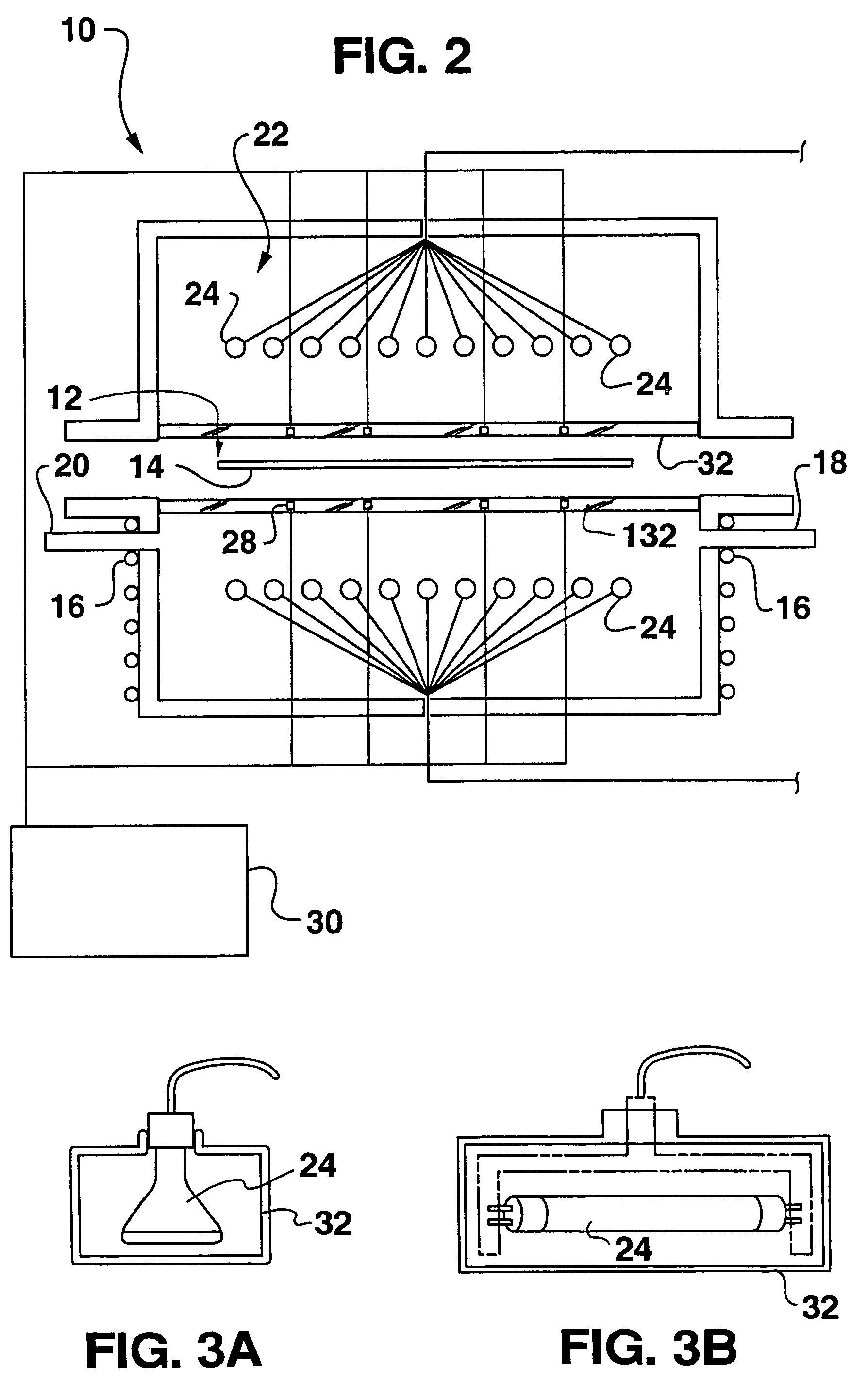
[0032]In general, the present invention is directed to an apparatus and method for heating semiconductor wafers while accurately monitoring the temperature of the wafer. The apparatus includes a thermal processing chamber in communication with a light source that is used to heat semiconductor wafers contained in the chamber. A radiation sensing device, such as a pyrometer, is in communication with the chamber and is positioned to sense thermal radiation at a particular wavelength being emitted by a semiconductor wafer. By sensing the thermal radiation being emitted by the wafer at a particular wavelength, the pyrometer can be used to calculate the temperature of the wafer during operation of the thermal p...


PUM

PropertyMeasurementUnit
wavelengthaaaaaaaaaa
wavelengthsaaaaaaaaaa

Abstract

A method and apparatus for heating semiconductor wafers in thermal processing chambers. The apparatus includes a non-contact temperature measurement system that utilizes radiation sensing devices, such as pyrometers, to determine the temperature of the wafer during processing. The radiation sensing devices determine the temperature of the wafer by monitoring the amount of radiation being emitted by the wafer at a particular wavelength. In accordance with the present invention, a spectral filter is included in the apparatus for filtering light being emitted by lamps used to heat the wafer at the wavelength at which the radiation sensing devices operate. The spectral filter includes a light absorbing agent such as a rare earth element, an oxide of a rare earth element, a light absorbing dye, a metal, or a semiconductor material.

Description

RELATED APPLICATIONS[0001]The present application is a continuation of U.S. patent application Ser. No. 10 / 288,271 filed on Nov. 5, 2002 and issued as U.S. Pat. No. 6,835,914.BACKGROUND OF THE INVENTION[0002]A thermal processing chamber refers to a device that uses energy, such as radiative energy, to heat objects, such as semiconductor wafers. Such devices typically include a substrate holder for holding a semiconductor wafer and a light source that emits light energy for heating the wafer. For monitoring the temperature of the semiconductor wafer during heat treatment, thermal processing chambers also typically include radiation sensing devices, such as pyrometers, that sense the radiation being emitted by the semiconductor wafer at a selected wavelength. By sensing the thermal radiation being emitted by the wafer, the temperature of the wafer can be calculated with reasonable accuracy.[0003]One major problem in the design of rapid thermal processing chambers having an optical tem...

Claims


Application Information

Patent Timeline
Patent Type & Authority Patents(United States)
IPC IPC(8): F27B5/14H01L21/00
CPCF27B5/04F27B17/0025H01L21/67115H01L21/67248H01L21/02H01L21/324
Inventor TIMANS, PAUL JANIS
Owner MATTSON TECHNOLOGY
Why Eureka
Try Eureka