Photomultiplier and radiation detector

a radiation detector and multi-layer technology, applied in the field of photomultipliers and radiation detectors, can solve the problems positional precision, flatness, levelness, etc., and achieve the effect of low resistance to vibration

Active Publication Date: 2006-11-14
HAMAMATSU PHOTONICS KK
View PDF7 Cites 9 Cited by
  • Summary
  • Abstract
  • Description
  • Claims
  • Application Information

AI Technical Summary

Benefits of technology

[0006]The former arrangement (the arrangement illustrated in FIG. 1 of Japanese Published Unexamined Patent Application No. Hei 5-290793) requires hermetic glass of a number corresponding to the number of stem pins and a step of setting each of these portions at a stem pin insertion position along with each stem pin. The number of parts and the number of manufacturing steps are thus large, and furthermore, since the anode and the electron multiplier unit are layered above the plurality of stem pins, the resistance against vibration is low and, for example, the hermetic glass becomes chipped due to mechanical stress applied to the stem pins.

Problems solved by technology

The number of parts and the number of manufacturing steps are thus large, and furthermore, since the anode and the electron multiplier unit are layered above the plurality of stem pins, the resistance against vibration is low and, for example, the hermetic glass becomes chipped due to mechanical stress applied to the stem pins.
Though improvements are thus made in regard to the issues of the former arrangement, since the tapered hermetic glass and the respective stem pins are generally joined by fusing by the melting of the hermetic glass, the respective surfaces (the upper and lower surfaces in the figure) of the stem formed of hermetic glass are low in positional precision, flatness, and levelness and thus give rise to the following issues.
That is, due to the lowering of the positional precision, flatness, and levelness of the inner surface (upper surface) of the stem, the positional precision of the interval between the electron multiplier unit, which is installed on the inner surface of the stem, and the photoelectric surface is degraded, causing degradation of characteristics and lowering of the seating property of the electron multiplier unit.

Method used


Image

  • Photomultiplier and radiation detector
  • Photomultiplier and radiation detector
  • Photomultiplier and radiation detector

Examples


Embodiment Construction

[0035]Preferred embodiments of this invention's photomultiplier and radiation detector shall now be described with reference to the drawings. The terms, “upper,”“lower,” etc., in the following description are descriptive terms based on the states illustrated in the drawings. In the drawings, portions that are the same or correspond to each other are provided with the same symbol and overlapping description shall be omitted.

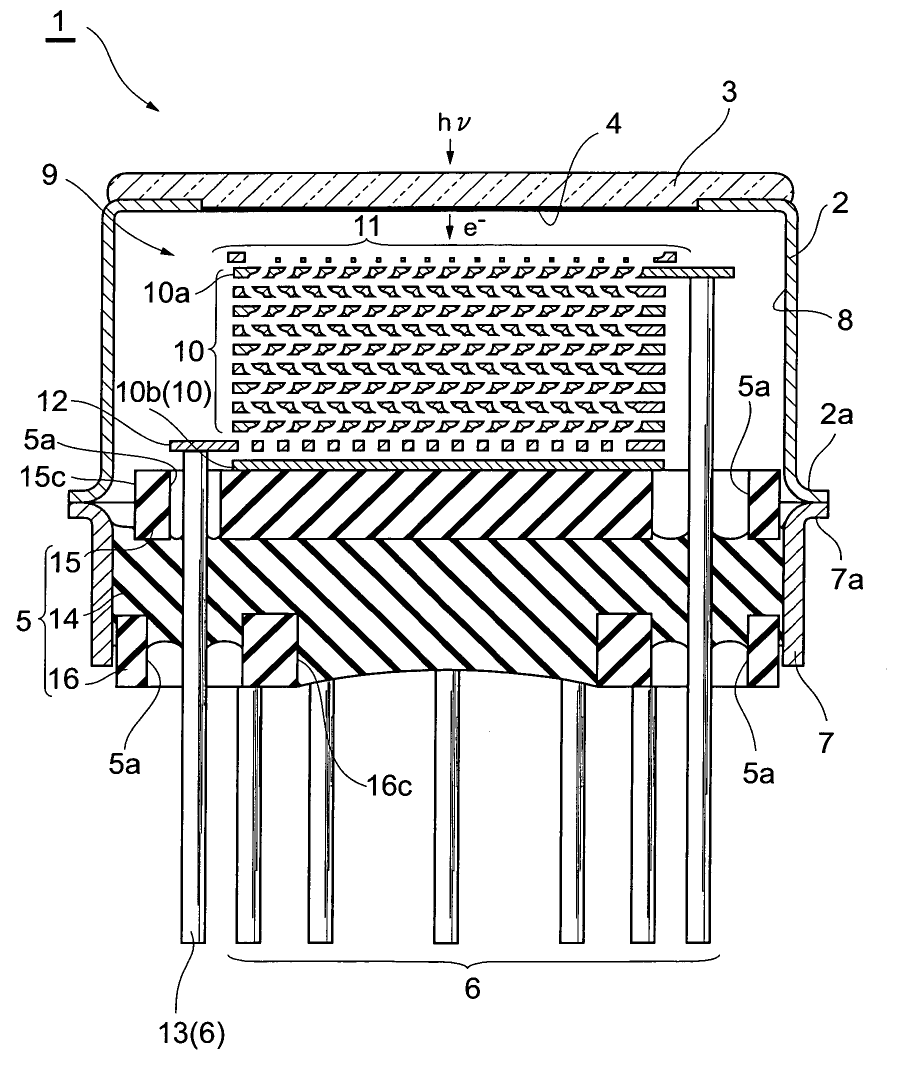
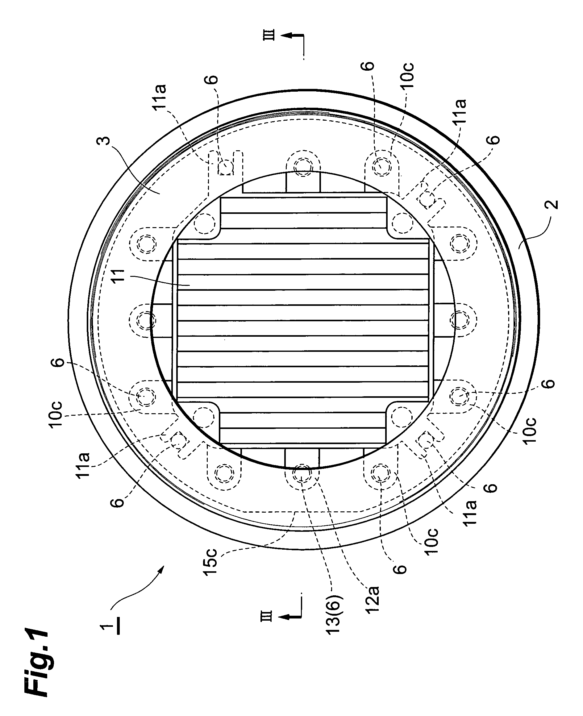
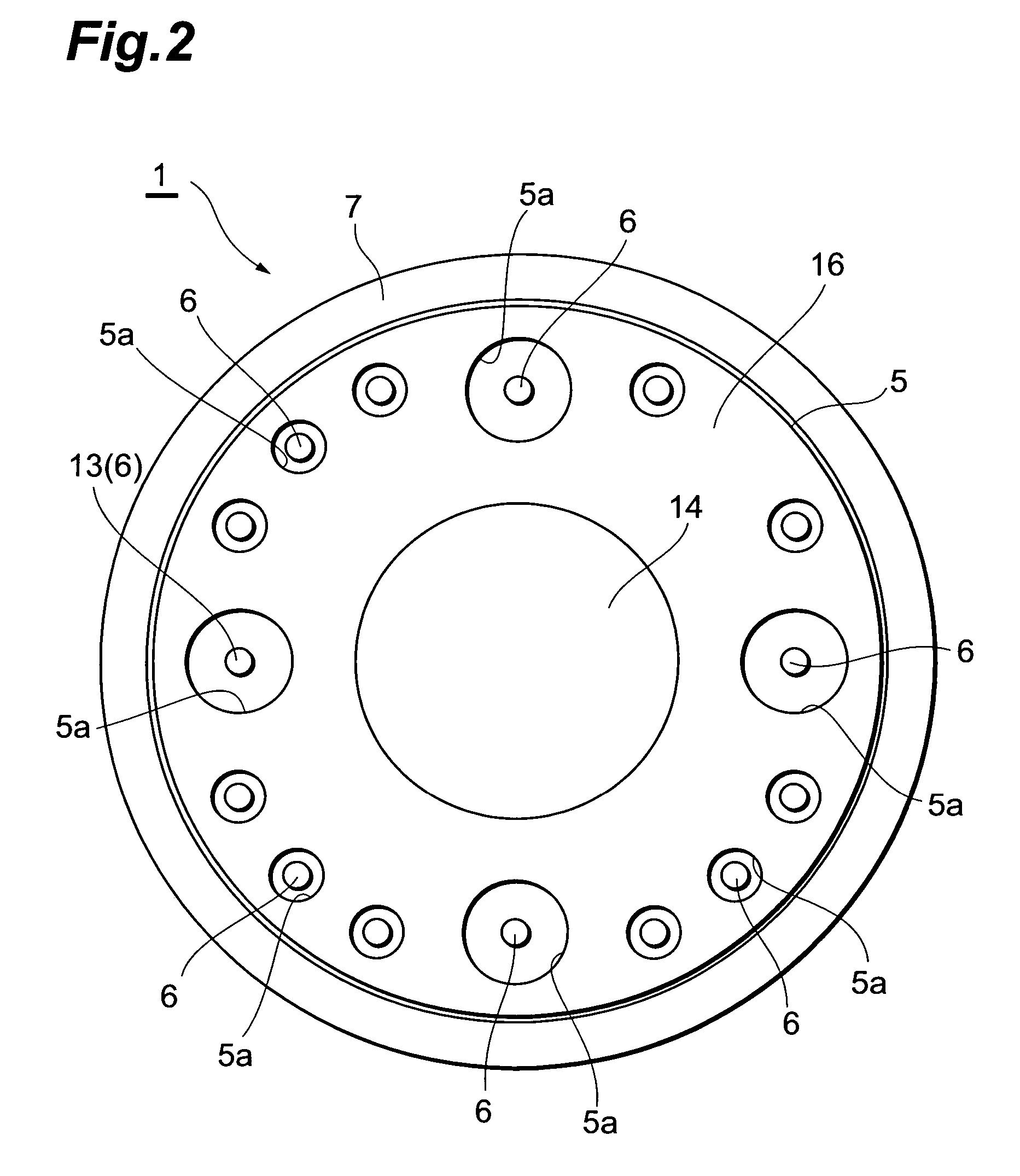
[0036]FIG. 1 and FIG. 2 are a plan view and a bottom view, respectively, of an embodiment of a photomultiplier by this invention, and FIG. 3 is a sectional view taken along line III—III in FIG. 1. In FIG. 1 to FIG. 3, a photomultiplier 1 is arranged as a device that emits electrons upon incidence of light from the exterior and multiplies and outputs the electrons as a signal.

[0037]As shown in FIG. 1 to FIG. 3, the photomultiplier 1 has a metal side tube 2 with a substantially cylindrical shape. As shown in FIG. 3, a glass light receiving plate 3 is fixed in an air...


PUM


Abstract

Onto a base member, through which stem pins are passed and holding members are to be joined to the respective surfaces thereof, the stem pins and the holding members are joined by fusion by melting of the base member to arrange a stem with at least three or more layers formed by sandwiching the base member by the holding members. In comparison to a conventional arrangement wherein the stem is arranged as a single layer of glass material and this is melted to fuse the stem pins, the positional precision, flatness, and levelness of both surfaces of the stem are improved.

Description

BACKGROUND OF THE INVENTION[0001]1. Field of the Invention[0002]This invention concerns a photomultiplier that makes use of the photoelectric effect and a radiation detector that uses this photomultiplier.[0003]2. Related Background of the Invention[0004]As one type of photomultiplier, a so-called head-on photomultiplier is known. With this head-on photomultiplier, a sealed vacuum container is arranged by providing a light receiving plate at an end portion at one side of a cylindrical side tube and providing a stem at an end portion at the other side of the side tube, and a photoelectric surface is disposed on the inner surface of the light receiving plate. An arrangement is provided wherein an electron multiplier unit, with a plurality of stages of dynodes, and an anode are layered and positioned opposite the photoelectric surface, and a plurality of stem pins, respectively connected to the respective dynodes and the anode, are insertedly mounted in the stem so as to lead to the ex...

Claims


Application Information

Patent Timeline
Patent Type & Authority Patents(United States)
IPC IPC(8): H01J21/20H01J43/04
CPCH01J43/28
Inventor SHIMOI, HIDEKIKYUSHIMA, HIROYUKI
Owner HAMAMATSU PHOTONICS KK
Why Eureka
Try Eureka