Non-volatile flash memory device

a non-volatile, memory device technology, applied in semiconductor devices, electrical devices, instruments, etc., can solve the problems of interrupting the reading of other cells along the bit line, radically deteriorating the endurance characteristic of the sonos device, and affecting the retention characteristic of the memory device, so as to achieve efficient and effective program/erase operations

Inactive Publication Date: 2006-11-14
DSS TECH MANAGEMENT +1
View PDF9 Cites 7 Cited by
  • Summary
  • Abstract
  • Description
  • Claims
  • Application Information

AI Technical Summary

Benefits of technology

[0016]A primary object of the present invention is to efficiently and effectively perform program / erase operations with a device having a sidewall floating gate which can control two bits with only one transistor.

Problems solved by technology

However, the thin thickness of the tunnel oxide may detrimentally affect the retention characteristic of the memory device.
However, the above-described method radically deteriorates the endurance characteristic of the SONOS device.
In other words, just one over-erased cell in the bit line may induct excessive current into the bit line and, therefore, interrupt reading data of other cells along the bit line.
Such over-erase may be caused by various structural problems such as a critical dimension in the cell of the flash memory, the thickness of the tunneling oxide layer, a junction overlap, the critical dimension of the floating gate, unevenness of the surface of the floating gate, the thickness of the ONO layer, the damage of the tunneling oxide layer, and pin holes.
However, detecting the over-erased cell is a time-consuming job and, additionally, complicated circuits are required to recover the detected over-erased cell.
Moreover, the threshold voltage distribution during the erase operation is wide and affects the threshold voltage distribution of a later program operation.
Consequently, the threshold window voltage decreases and a multi-level bit is difficult to achieve in accordance with the conventional art methods.

Method used


Image

  • Non-volatile flash memory device
  • Non-volatile flash memory device
  • Non-volatile flash memory device

Examples


Embodiment Construction

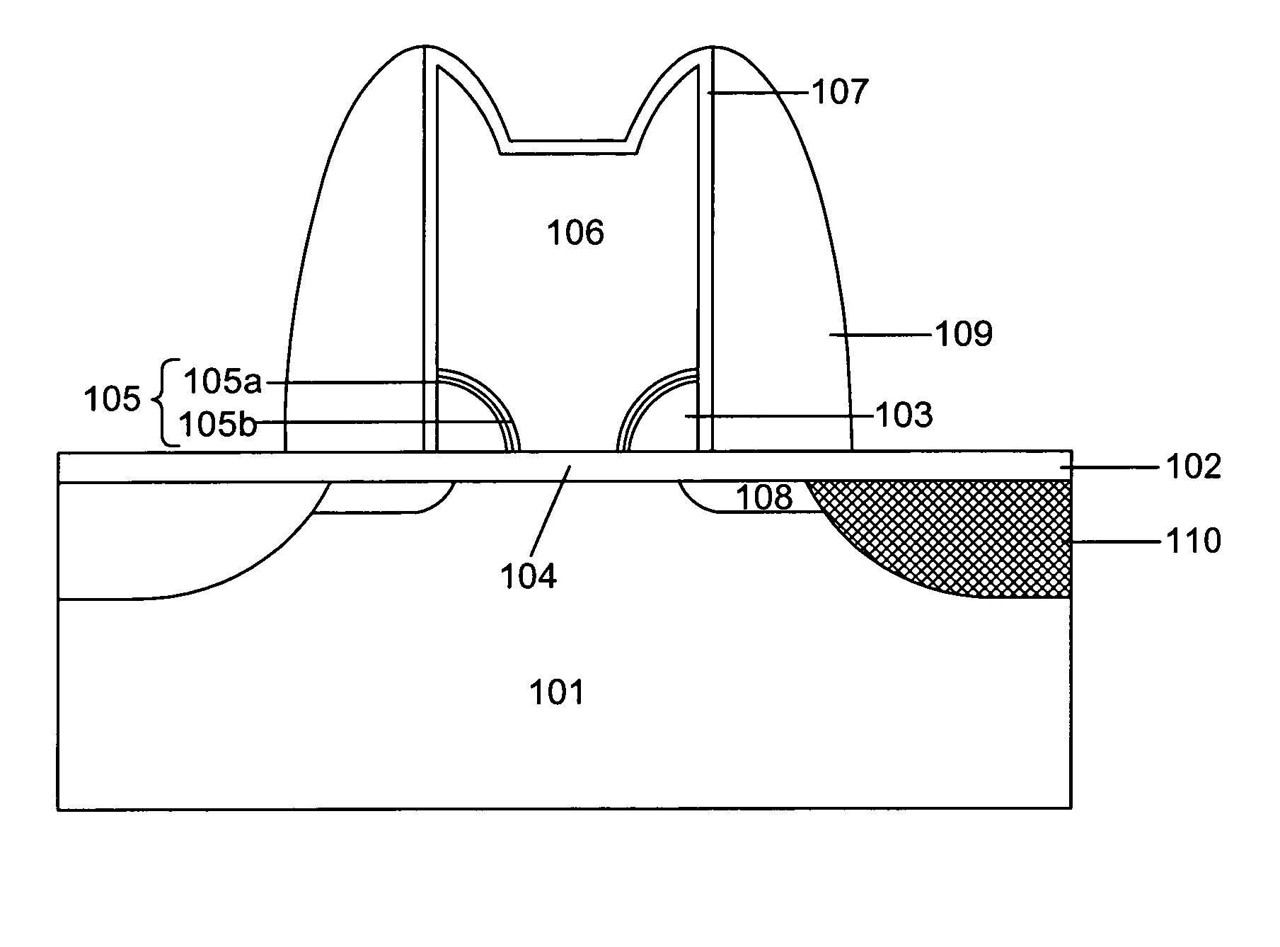
[0026]FIG. 3 is a cross-sectional view illustrating a non-volatile memory device having a sidewall floating gate which can control two bits with one transistor in accordance with the present invention.

[0027]Referring to FIG. 3, a gate oxide layer 104 is grown on a semiconductor substrate 101. A polysilicon gate 106 is positioned on the gate oxide layer 104. Sidewall floating gates 103 are placed on the bottom of the lateral faces of the polysilicon gate 106. Block oxide layers 105 is placed between the polysilicon gate 106 and the sidewall floating gates 103. The block oxide layers 105 comprise first block oxide layers 105a and second block oxide layers 105b. The first block oxide layers 105a have a thickness ranging between 50 Å and 250 Å and are made of a material selected from the group consisting of Al2O3 and Y2O3. The second block oxide layers 105b preferably have a thickness ranging between 20 Å and 150 Å and are made of SiO2. A tunnel oxide layer 102 is positioned between the...


PUM


Abstract

A non-volatile memory device having sidewall floating gates implementing two bits with just one transistor is disclosed. A disclosed method comprises a non-volatile memory device having a unit cell comprising: a transistor including a polysilicon gate, sidewall floating gates, block oxide layers and source and drain regions; a word line vertically placed on a substrate and connected to the polysilicon gate; and a pair of bit lines orthogonally placed to the word line and connected to the source and drain regions.

Description

BACKGROUND OF THE INVENTION[0001]1. Field of the Invention[0002]The present disclosure relates generally to a semiconductor fabrication and, more particularly, to a non-volatile memory device having sidewall floating gates which can control two bits with just one transistor.[0003]2. Background of the Related Art[0004]In general, there are two categories in semiconductor devices, namely, a volatile memory and a non-volatile memory. The volatile memory again includes a dynamic random access memory (hereinafter referred to as “DRAM”) and a static DRAM (hereinafter referred to as “SDRAM”). One characteristic of the volatile memory is that data are maintained just while electric power is being applied. In other words, when power is turned off, the data in the volatile memory disappear. On the other hands, the non-volatile memory, mainly a ROM (Read Only Memory), can keep the data regardless of the application of electric power.[0005]From the point of a view of the fabrication process, th...

Claims


Application Information

Patent Timeline
Patent Type & Authority Patents(United States)
IPC IPC(8): H01L29/788H01L27/115G11C16/04
CPCG11C16/0458H10B69/00
Inventor JUNG, JIN HYO
Owner DSS TECH MANAGEMENT
Why Eureka
Try Eureka