Organic thin-film transistor and method of manufacturing the same

a thin-film transistor and organic technology, applied in transistors, solid-state devices, thermoelectric devices, etc., can solve the problems of unsuitable mass-production, difficult to obtain a short source-drain distance of or below 10 m, and a superior technique has yet to be established, and achieves short channel length, easy manufacturing, and good control

Inactive Publication Date: 2006-11-21
NAT INST OF ADVANCED IND SCI & TECH
View PDF25 Cites 11 Cited by
  • Summary
  • Abstract
  • Description
  • Claims
  • Application Information

AI Technical Summary

Benefits of technology

[0029]Since the organic thin-film transistor of the invention is composed of organic semiconductor thin film, by adapting the thin-film thickness to the distance between the source and the drain, an extremely short channel length can be precisely formed without using high-level fine processing technology.
[0030]Also, because the transistor device structure is composed of thin-film layers, printing technology can be adapted and it can be readily manufactured with good control.
[0031]Also, leakage current between the source and the drain can be reduced through the formation of the source and the drain from materials having different work functions.

Problems solved by technology

Although various techniques have been studied up until now, the problem is that a superior technique has yet to be established.
A problem with this method is that, so long as an ordinary mask is used, it is difficult to obtain a short source-drain distance of or below 10 μm.
Another problem is that when a special mask is used that can be adapted to fine processing a single fabrication of an electrode clogs the mask, making it unsuitable for mass-fabrication.
However, in order to thus apply the technology, the semiconductor layers of the thin-film transistor are composed of organic material, which makes it difficult to introduce the operation of washing off the photo-mask with an organic solvent.
Moreover, even if manufacturing processes were to be devised to which photolithography could be adapted, thereby enabling the performance provided by a thin-film transistor to be utilized, when the cost and time requirements of the photolithography technology are taken into consideration, it becomes impossible to achieve the low-cost, low-energy production that characterizes the use of organic material for thin-film transistors.
However, a problem with this technology is that it requires the adapting of electron beam lithography, which, being an extremely high-level, costly technology, means that the characterizing ability to adapt a simple, convenient process, such as printing or the like, provided by the use of organic material for thin-film transistors, is not achieved.
Another problem is that of reduced throughput.
However, a problem with the technology is that the channel length depends on the width of the spacers, which necessarily means a reliance on fine-processing technology for how fine the spacers can be manufactured.
Another problem is that although source-drain fabrication is easy, it is extremely difficult to fabricate the gate electrode.
It has been difficult to fabricate low-cost, high performance devices with these methods, due to the very high level and high cost of the adapted fine processing technologies.
Furthermore, drastically reducing the channel length has given rise to a problem in terms of the transistor characteristics, caused by an increase in the leakage current between the source and the drain that has made it impossible to obtain a large current amplification ratio (on / off ratio).

Method used


Image

  • Organic thin-film transistor and method of manufacturing the same
  • Organic thin-film transistor and method of manufacturing the same
  • Organic thin-film transistor and method of manufacturing the same

Examples


example 1

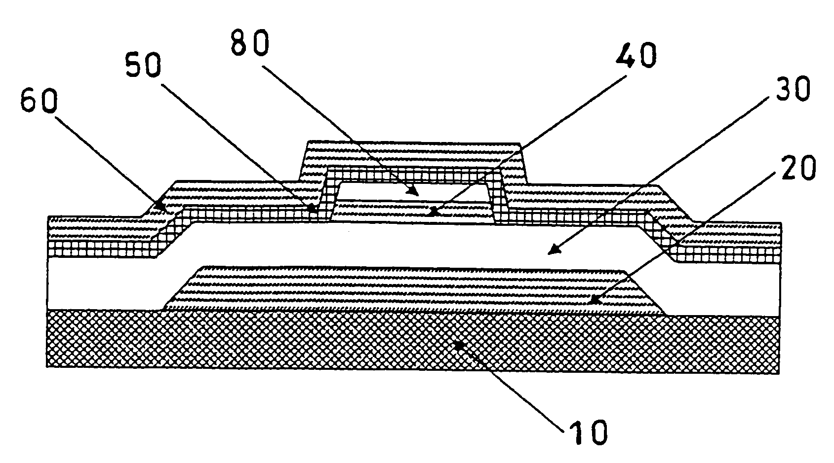
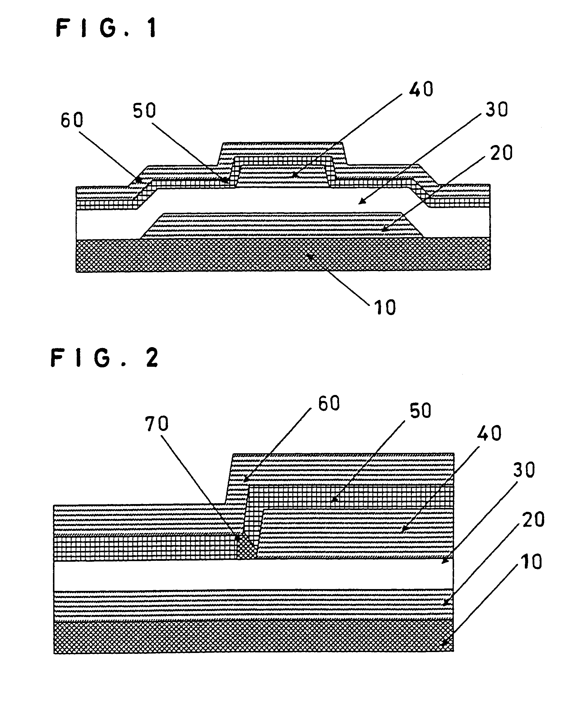
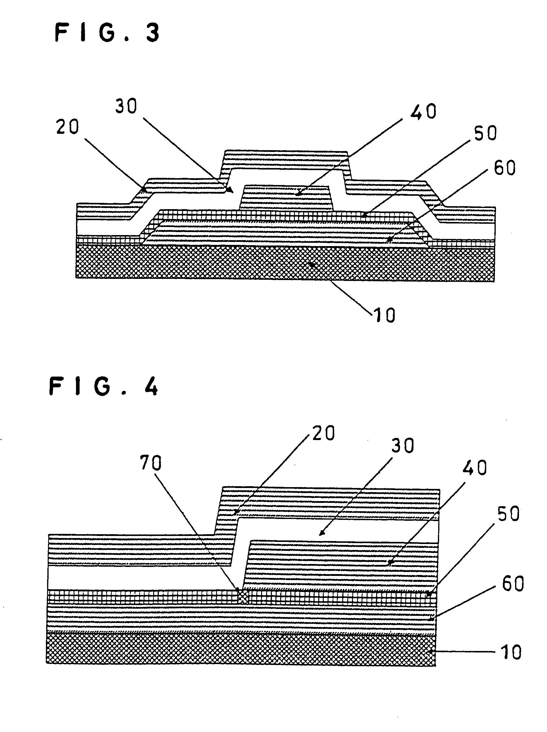
[0096]A substrate (area: 20×35 mm, thickness: 1.0 mm) of synthetic quartz (ES grade) was subjected to 20 minutes of ultrasonic washing with a neutral detergent (PureSoft produced by Iuchi Seieidou Co.) diluted five-fold with pure water, followed by 20 minutes of ultrasonic washing in pure water to remove the detergent. An ultraviolet light-ozone washing device was then used to wash the substrate for 20 minutes by irradiating it with ultraviolet light in an oxygen atmosphere. A nickel mask was then utilized to vacuum-deposit gold onto the quartz substrate thus washed to form a gate electrode 20 that was 100-μm wide and 0.2-μm thick. The film formation conditions at this time were a deposition rate of 6 nm a minute with the substrate at 30° C. Next, as shown in FIG. 12, polymethyl methacrylate (PMMA) was dissolved in chloroform and the solution was used to form on the top of the gate electrode 20 the insulation layer 30 as a layer 0.4-μm thick, using the spin-coating method. Then, as ...

example 2

[0097]An n-type silicon substrate (area: 20×35 mm, thickness: 1.0 mm) on which a 300-nm thermally oxidized silicon film was grown to form an insulation layer 30, was subjected to 20 minutes of ultrasonic washing with a neutral detergent (PureSoft produced by Iuchi Seieidou Co.) diluted five-fold with pure water, followed by 20 minutes of ultrasonic washing in pure water to remove the detergent. An ultraviolet light-ozone washing device was then used to wash the substrate for 20 minutes by irradiating it with ultraviolet light in an oxygen atmosphere. A nickel mask was then utilized to vacuum-deposit onto the substrate thus washed, a gold drain 40 that was 100-μm wide and 0.2-μm thick. The film formation conditions at this time were a deposition rate of 6 nm a minute at a substrate temperature of 30° C. On the top thereof, for the semiconductor layer 50, the vacuum-deposition method was used to form a pentacene thin-film. Refined pentacene was used that had been sublimation-refined t...

example 3

[0098]An n-type silicon substrate (area: 20×35 mm, thickness: 1.0 mm) on which a 300-nm thermally oxidized silicon film was grown to form an insulation layer 30, was subjected to 20 minutes of ultrasonic washing with a neutral detergent (PureSoft produced by Iuchi Seieidou Co.) diluted five-fold with pure water, followed by 20 minutes of ultrasonic washing in pure water to remove the detergent. An ultraviolet light-ozone washing device was then used to wash the substrate for 20 minutes by irradiating it with ultraviolet light in an oxygen atmosphere. A nickel mask was then utilized to vacuum-deposit onto the substrate thus washed, a gold drain 40 that was 100-μm wide and 0.2-μm thick. The film formation conditions at this time were a deposition rate of 6 nm a minute at a substrate temperature of 30° C. On the top thereof, for the semiconductor layer 50, the vacuum-deposition method was used to form a pentacene thin-film. Refined pentacene was used that had been sublimation-refined t...


PUM

PropertyMeasurementUnit
thicknessaaaaaaaaaa
angleaaaaaaaaaa
angleaaaaaaaaaa

Abstract

A thin-film transistor includes a substrate (10), a gate electrode (20) provided on a portion of the substrate, an insulation layer (30) arranged to cover the gate electrode and the substrate, a source or drain (40) provided on the insulation layer in a region corresponding to a region of the gate electrode, a semiconductor layer (50) arranged to cover the source or drain (40) and the insulation layer, a drain or source (60) provided on the semiconductor in a portion of a region corresponding to a region of the source or drain (40) that overlaps with the gate electrode, and a channel (70) formed between the source or drain (40) and the drain or source (60) and having a length defined by a film thickness of the semiconductor layer (50).

Description

TECHNICAL FIELD[0001]The present invention relates to a thin-film transistor. More particularly, the invention relates to an organic thin-film transistor which uses an organic semiconductor as a semiconductor layer to improve thin-film transistor characteristics and which can also be fabricated using a simple, convenient process, such as printing or the like, and to a method of manufacturing the same.BACKGROUND ART[0002]In recent years, various integrated circuit technologies have been proposed that use organic semiconductor thin-film transistors. It is expected that it will be possible to fabricate such integrated circuits by a simple, convenient manufacturing method, such as printing technology or the like, while other advantages include the possibility of realizing large-area processing and low-cost manufacturing processes, and good compatibility for fabrication on flexible substrates. This is also attracting expectations for the good compatibility with integrated circuit technol...

Claims


Application Information

Patent Timeline
Patent Type & Authority Patents(United States)
IPC IPC(8): H01L29/786H01L27/105H01L21/8246H01L21/8247H01L29/788H01L29/792H01L51/00H01L51/05H01L51/30
CPCH01L51/0545H01L51/057H01L51/0036H01L51/0052H01L51/0516H10K85/113H10K85/615H10K10/468H10K10/491H10K10/466
Inventor KAMATA, TOSHIHIDEYOSHIDA, MANABU
Owner NAT INST OF ADVANCED IND SCI & TECH
Why Eureka
Try Eureka