High dynamic range charge readout system

a charge readout and high dynamic range technology, applied in the field of solid state image sensors, can solve the problems of impact ionization, noise floor of the present day charge conversion amplifier is approximately 10 electrons, and cannot be easily reduced, and achieve the effect of high dr, low noise floor, and low pulse amplitud

Inactive Publication Date: 2006-11-21
ISETEX
View PDF6 Cites 26 Cited by
  • Summary
  • Abstract
  • Description
  • Claims
  • Application Information

AI Technical Summary

Benefits of technology

[0008]The present invention defines structure in CCDs that overcome limitations in the prior art. The invention provides a practical high DR readout system in which the DR is not restricted by the voltage swing limitations on the charge detection node. It defines a practical high performance image sensors of various architectures that have high DR. These structural advances are achieved by incorporating Charge Multiplier cells into a horizontal register of a CCD image sensor. As the charge is multiplied, the horizontal register is correspondingly increased in width and more charge multiplication gates are added per stage. A charge overflow region then follows the charge multiplier. In this region the amount of charge that exceeds a certain predetermined threshold is split off into another register. A detection node that has different conversion sensitivity may terminate this register. The process of charge overflow and splitting off can continue for more that two steps. As a result, the dynamic range of the sensor can be almost arbitrarily compressed with a predetermined charge to voltage transfer characteristic directly in the charge domain. Charge domain DR compression allows full utilization of the high DR obtained by the charge multiplier without imposing stringent demands on the DR of charge detection nodes and amplifiers. Finally, the orientation of charge multiplying registers themselves with respect to certain crystallographic directions of the semiconductor substrate are optimized for minimum pulse amplitude and minimum noise.

Problems solved by technology

The suitable clocking voltages generate high fields in the structure and when a carrier is injected into these high field regions, it gains energy and may cause impact ionization.
The noise floor of the present day charge conversion amplifiers is approximately 10 electrons, and cannot be easily reduced.
Charge multiplication, however, presents a problem for the design of the CCD registers.
This may not be easily accomplished in the registers that are restricted in both dimensions by the sensor pixel size.
A second problem resulting from charge multiplication is related to the DR of charge conversion structures at the input of the charge detection amplifier.
However, when the charge is multiplied, the voltage increment may be so large that the detection node cannot handle it.
The available maximum voltage swing thus unduly limits the DR of the sensor.
The prior art also does not teach how to design a charge readout system that has high DR and that is not restricted by the maximum allowable voltage swing on the charge detection node.

Method used


Image

  • High dynamic range charge readout system
  • High dynamic range charge readout system
  • High dynamic range charge readout system

Examples


Embodiment Construction

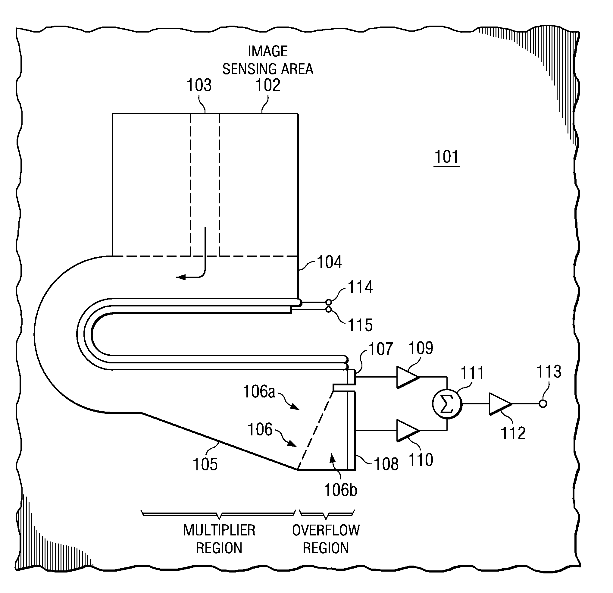
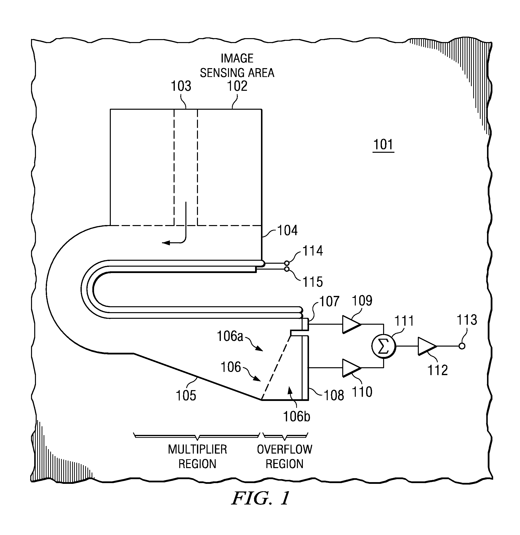
[0016]In FIG. 1, a plan view of a typical CCD area image sensor architecture is shown. The semiconductor substrate is indicated as the region 101 where the active areas of the sensor are enumerated. The region 102 is the active image sensing area that is divided into individual pixels by channel stops and transfer gates. Both the channel stops and the gates are not shown to simplify the drawing.

[0017]There are many types of image sensor architectures ranging from Frame Transfer to Interline Transfer with single horizontal register or multiple registers that can be used here. However, these options will not be discussed here any further to simplify the description. It is clear to those skilled in the art that the present invention can apply to all of them.

[0018]The region 103 in FIG. 1 represents one vertical column of pixels that interfaces with the horizontal register 104. When the image area gates are clocked, the charge from one row of pixels is transferred into the horizontal re...


PUM


Abstract

A solid-state image sensor has a readout architecture that incorporates charge multiplier cells into a horizontal register of a CCD image sensor, and includes a first CCD register adjacent to at least a second CCD register and coupled to the said first register through a charge overflow barrier. A high Dynamic Range readout system results in which the DR is not restricted by the voltage swing limitations on the charge detection node. As the charge is multiplied, the horizontal register structure increases in width and more charge multiplication gates are added per stage. A charge overflow region follows the charge multiplier. In this region the amount of charge that exceeds a certain predetermined threshold is split off into another register. A detection node that has different conversion sensitivity may terminate this register. The process of charge overflow and splitting off may continue for more than two steps.

Description

FIELD OF THE INVENTION[0001]The invention relates to solid-state image sensors, and more particularly to image sensors that have a readout architecture that incorporates charge multipliers that have high DR with large charge handling capabilities, and that extends the charge Dynamic Range (DR) of the sensor thus increasing the demand on the DR of charge readout systems.DESCRIPTION OF RELATED ART[0002]A typical image sensor senses light by converting impinging photons into electrons that are integrated (collected) in sensor pixels. After the integration cycle is completed, the charge is converted into a voltage that is supplied to the output terminals of the device. Charge to voltage conversion is accomplished either directly in the sensor pixels, such as in the Active Pixel CMOS image sensors, or remotely off the sensing area, in charge conversion amplifiers. In the remote conversion approach, the charge must be transported to the sensing amplifier by a well know charge transferring...

Claims


Application Information

Patent Timeline
Patent Type & Authority Patents(United States)
IPC IPC(8): H04N5/335H01L27/148H04N5/355H04N5/357H04N5/359H04N5/372H04N5/376H04N5/378
CPCH01L27/14806H01L27/14831H01L27/14887H04N5/243H04N5/357H04N5/3595H04N5/37213H04N23/76H04N25/625H04N25/60H04N25/713
Inventor HYNECEK, JAROSLAV
Owner ISETEX
Why Eureka
Try Eureka