High dynamic range active pixel CMOS image sensor and data processing system incorporating adaptive pixel reset

a high dynamic range, active pixel technology, applied in the field of solid state image sensors and imaging systems, can solve the problems of limiting the dr of the sensor, the disadvantage of shooting and rolling shutter scanning modes, etc., and achieve the effect of improving the sensor performance and high dr

Active Publication Date: 2006-07-18
INTELLECTUAL VENTURES II
View PDF11 Cites 47 Cited by
  • Summary
  • Abstract
  • Description
  • Claims
  • Application Information

AI Technical Summary

Benefits of technology

[0008]The present invention provides practical and simple CMOS image sensor architecture that allows for individual pixel resets based on the amount of integrated charge in each pixel. By incorporating additional horizontal register into the sensor chip that stores the row pixel reset information, it is possible to selectively skip the reset for pixels that are dimly illuminated. The high DR image sensors are capable of resolving image details simultaneously in both; highly illuminated as well as in the dark areas of the image without loss of contrast or signal clipping. This significantly improves performance of the sensor, and achieves high DR and other objects of the invention.

Problems solved by technology

Both the snap shot and the rolling shutter scanning modes have a disadvantage in limiting the sensor DR.

Method used


Image

  • High dynamic range active pixel CMOS image sensor and data processing system incorporating adaptive pixel reset
  • High dynamic range active pixel CMOS image sensor and data processing system incorporating adaptive pixel reset
  • High dynamic range active pixel CMOS image sensor and data processing system incorporating adaptive pixel reset

Examples


Embodiment Construction

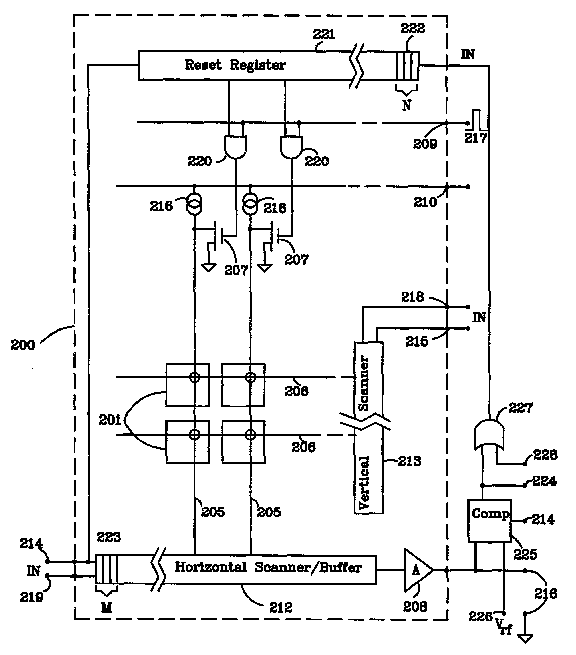
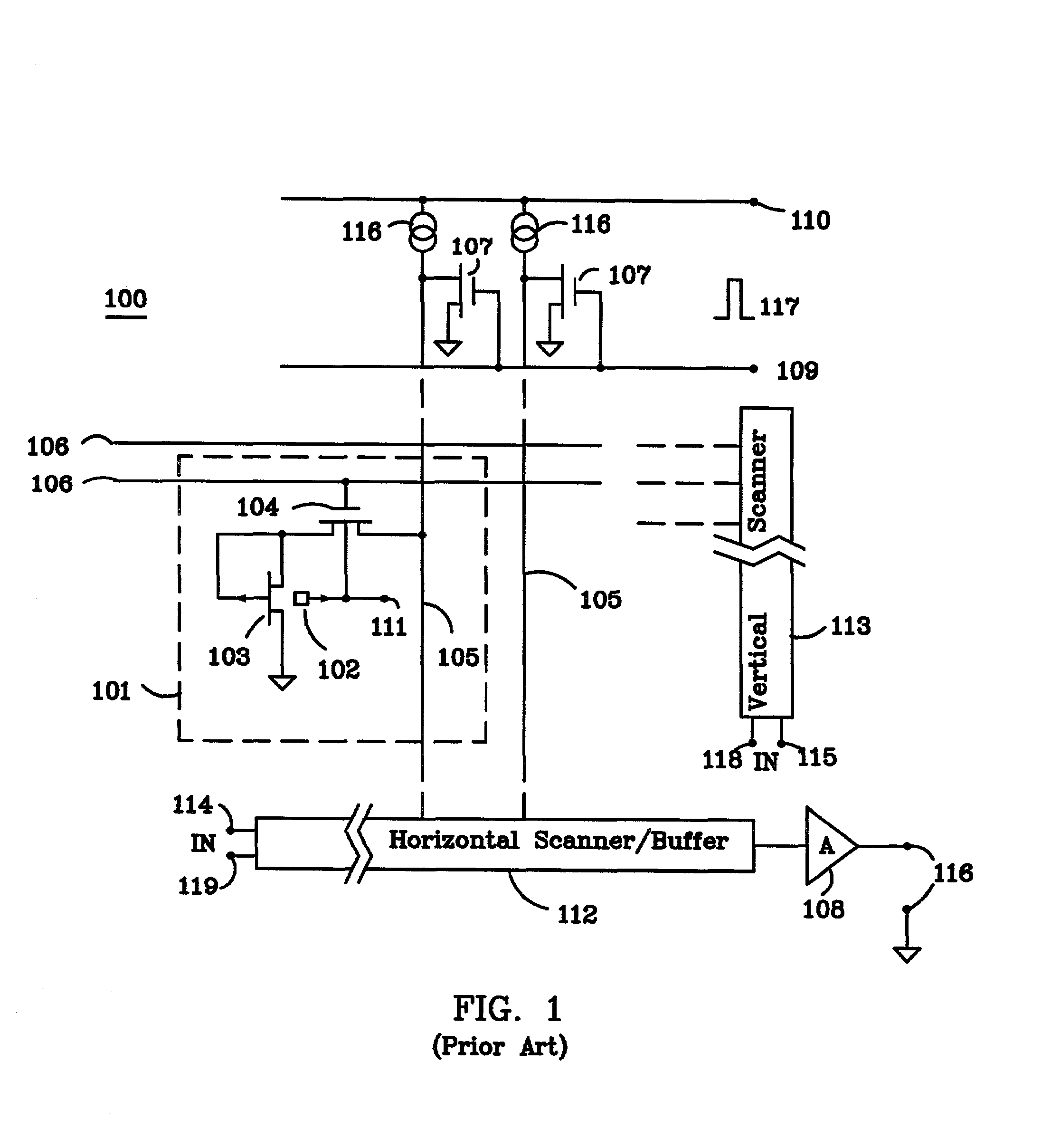
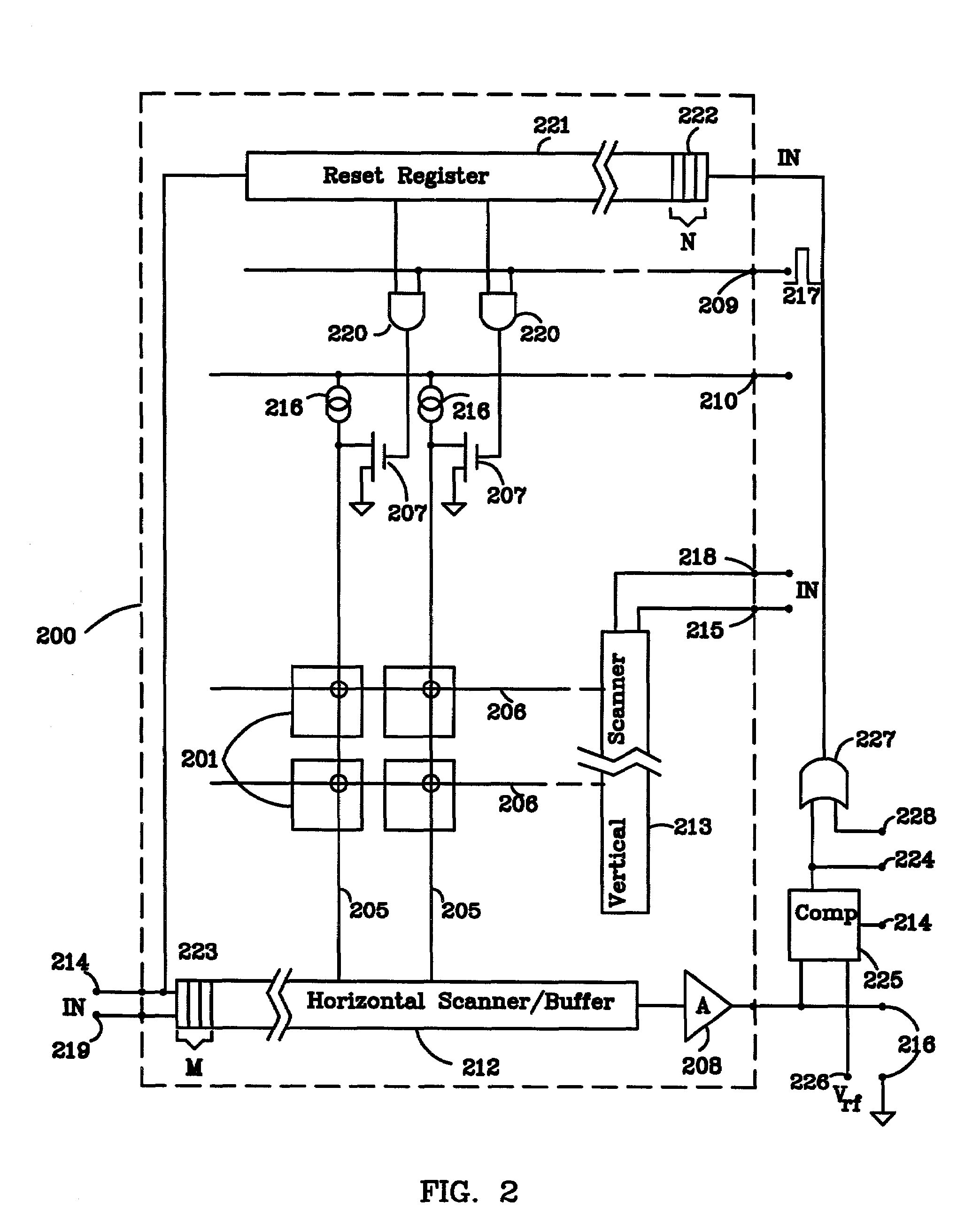
[0014]In FIG. 2, the block diagram of sensor 200 of the present invention is shown. The diagram also shows the details of the column sense line biasing circuits and the reset logic circuits. The pixels in one row are selectively reset depending on the data loaded into the reset register. The circuit is similar to the diagram of the sensor shown in FIG. 1 with the major additions being the reset register 221 and the reset logic gates 220. Pixels 201 are addressed as previously by row signals supplied through the lines 206 from the vertical scanner 213. Pulses applied to the register clocking input 215 clock the scanner and the scan is started by applying the starting pulse to terminal 218. The pixel signal is transferred on the vertical column lines 205, and further into the horizontal scanner-buffer 212. The pulses applied to the terminal 214 clock the horizontal scanner and the pulse applied to the terminal 219 starts the scan. M dummy stages 223 have been added to the beginning of...


PUM


Abstract

A high Dynamic Range Active Pixel CMOS image sensor architecture has incorporated therein an adaptive pixel reset. The individual sensor pixels are reset only when accumulated charge, or the integration time exceeds certain predetermined limits. The reset is skipped when the integrated charge signal in a given pixel is low. The accumulated number of reset skips in a given time frame, together with the standard analog output, is used to calculate the sensor high DR output signal. A signal processing system is used to simultaneously process both sensor analog and digital outputs.

Description

PRIORITY[0001]Priority is based upon Provisional application Ser. No. 60 / 269,554, filed Feb. 20, 2001.FIELD OF THE INVENTION[0002]The invention relates to solid-state image sensors and imaging systems, specifically to Active Pixel CMOS Image Sensors (APS) and imaging systems that have high Dynamic Range (DR) achieved by resetting the pixels of the array individually corresponding to the level of integrated charge.BACKGROUND OF THE INVENTION[0003]A typical image sensor senses light by converting impinging photons into electrons and collecting (integrating) them in sensor pixels. After the integration cycle is completed charge is converted into a voltage that is supplied to the output terminals of the sensor. An example of pixel circuit diagram (101) for an advanced active pixel CMOS image sensor array (100) is shown in FIG. 1. In this example, the charge to voltage conversion is accomplished by integrating charge in a special potential well 102 of a p-channel transistor 103 (U.S. pat...

Claims


Application Information

Patent Timeline
Patent Type & Authority Patents(United States)
IPC IPC(8): H04N5/228H01L27/146H04N5/355H04N5/374H04N5/376H04N5/378
CPCH04N3/155H04N25/533H04N25/583H04N25/76
Inventor HYNECEK, JAROSLAV
Owner INTELLECTUAL VENTURES II
Why Eureka
Try Eureka