Chip carrier for fingerprint sensor

a fingerprint sensor and chip carrier technology, applied in the field of biometric sensors, can solve the problems of increasing the likelihood of authentication being more difficult, affecting the accuracy of enrollment and authentication, and affecting the reliability of users, so as to improve the reliability of users and accurately position and sweep the fingers

Active Publication Date: 2006-12-05
FUJITSU SEMICON LTD
View PDF19 Cites 96 Cited by
  • Summary
  • Abstract
  • Description
  • Claims
  • Application Information

AI Technical Summary

Benefits of technology

[0006]In order to overcome these problems, the present invention is generally directed to structures and methods which assist users in accurately and consistently positioning their fingers on sweep-type fingerprint sensors prior to being read (i.e., prior to image capture), and which assist in moving the fingers across the sensor in the correct path.
[0007]The present invention comprises a self-aligning chip carrier having a recess for receiving and mounting a sweep-type fingerprint sensor with tactile elements formed or mounted on the upper surface of the carrier. The tactile elements may be used to position the finger prior to being read, and to guide the path of the finger as it is swept across the sensor. In one embodiment, the tactile elements comprise two generally parallel ridges formed or positioned adjacent to the sensor to help align the finger and to guide the finger as it is swept across the sensor. In another embodiment, a tactile element comprises a full or partial oval ridge having a major axis which is generally along the path of finger motion. The top of the oval, comprising an arcuate portion of the ridge, is used to position the tip of the finger prior to reading, and the sides

Problems solved by technology

If the image taken from the user during enrollment has limited or unrecognizable data points, either the enrollment will be rejected or, if accepted, there will be the increased likelihood that authentication will be more difficult due

Method used


Image

  • Chip carrier for fingerprint sensor
  • Chip carrier for fingerprint sensor
  • Chip carrier for fingerprint sensor

Examples


Embodiment Construction

[0022]To facilitate its description, the invention is described below in terms of specific embodiments and with reference to the Figures.

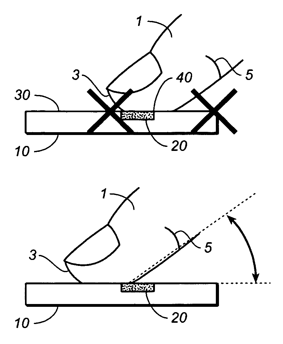
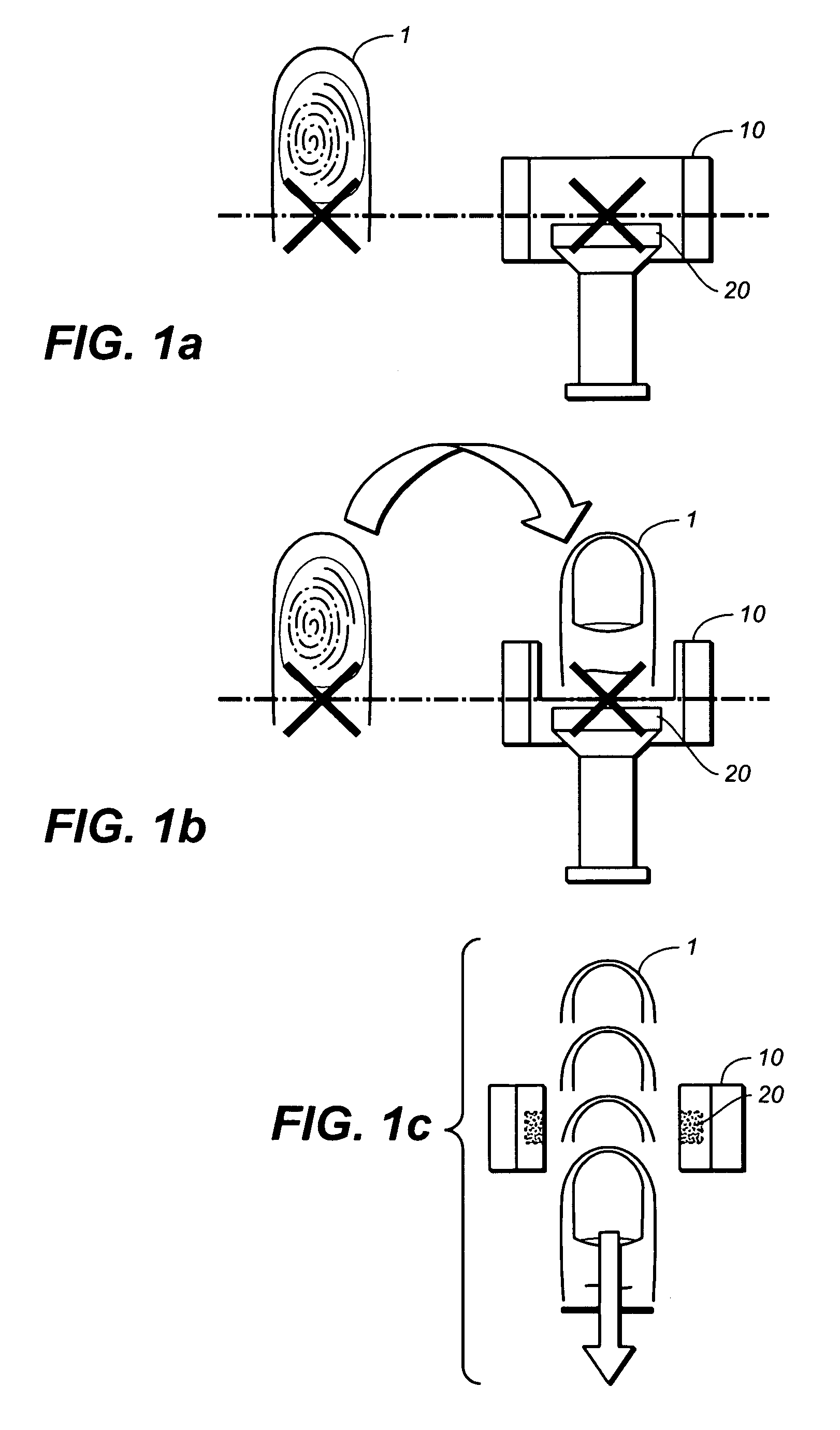
[0023]As discussed above, reliable fingerprint identification requires first the enrollment of an accurate fingerprint image which is captured and stored for later comparative purposes and, thereafter, accurate capturing of a user's fingerprint image for purposes of authentication. Both of these processes require the capturing of a high quality image, and consistency in the image capturing process. Turning to FIGS. 7a–7c, common errors in capturing images with a sweep-type sensor are depicted. Each of FIGS. 7a–7c show a finger 1 placed on a fingerprint sensor 20, held by a carrier 10. The upper surface 40 of sensor 20 is shown flush mounted with the upper surface 30 of carrier 10. In order to capture a high quality image, a substantial length of the finger 1, between the finger tip 3 and the first joint 5 should be swept across upper surface 40 of ...


PUM


Abstract

A carrier for a sweep-type fingerprint sensor and a method of operation are disclosed. The carrier has a recess for receiving and mounting the fingerprint sensor and one or more tactile elements for assisting the user in positioning a finger, and in correctly moving the finger across the sensor being read. In one embodiment the tactile element consists of an oval ridge, or a portion thereof, defining a major axis which is lies in the sweep direction. The tip of the finger is initially positioned in the arcuate portion of the oval ridge and is moved across the sensor, generally along the axis of the oval. The side walls of the ridge assist the user in correctly moving the finger across the sensor.

Description

CROSS REFERENCE TO RELATED APPLICATIONS[0001]This application is related to commonly owned U.S. patent application Ser. No. 10 / 160,438, entitled “System for Flexible Interconnect Packaging” and U.S. patent application Ser. No. 10 / 094,954, entitled “System for Providing an Open-Cavity Low Profile Encapsulated Semiconductor Package,” the disclosures of which are incorporated by reference.FIELD OF THE INVENTION[0002]The present invention relates to biometric sensors, and is particularly related to packaging for sweep-type fingerprint sensors, and methods for using such sensors.BACKGROUND OF THE INVENTION[0003]Devices and methods for biometric identification are becoming increasingly important for providing secure access to restricted areas or devices. Biometric sensing offers significant advantages over alternative methods of restricting access to sensitive areas and equipment to authorized users. Fingerprint sensing has become one of the most important biometric sensing techniques. Ho...

Claims


Application Information

Patent Timeline
IPC IPC(8): G06K9/00
CPCG06K9/00026G06V40/1335
Inventor MANANSALA, MICHAEL C.
Owner FUJITSU SEMICON LTD
Why Eureka
Try Eureka