Planar waveguide reflective diffraction grating

a reflective diffraction and waveguide technology, applied in the direction of optical multiplex, electrical apparatus, instruments, etc., can solve the problems of large phase difference between interfering paths, the incident beam is not in the direction, and the existing devices are limited to operation over small wavelength ranges

Inactive Publication Date: 2006-12-19
ENABLENCE
View PDF11 Cites 53 Cited by
  • Summary
  • Abstract
  • Description
  • Claims
  • Application Information

AI Technical Summary

Problems solved by technology

Higher orders result in deviation of the incident beam from the direction predicted by geometric (ray) optics.
In particular, advancements in Echelle gratings, which usually operate at high diffraction orders (40 to 80), high angles of incidence (approx 60°) and large grading pitches, have lead to large phase differences between interfering paths.
Thus, existing devices are limited to operation over small wavelength ranges due to the high diffraction orders required (see equation 5).
Furthermore, for diffraction grating-based devices fabricated in a planar waveguide platform, a common problem encountered in the prior art is polarization dependent loss arising from field exclusion of one polarization caused by the presence of conducting metal S (a reflective coating) adjacent to the reflective facets F.
Ultimately, the presence of sidewall metal manifests itself in the device performance as polarization-dependent loss (PDL).
This solution can be of limited utility because it requires limitations on election of blaze angles and blaze wavelength.
This solution is also of limited utility because it requires reflective coating on some of the surfaces but not the others, leading to additional manufacturing steps requiring selective treatment of the reflecting interfaces.
It has long been thought that gratings with a small diffraction order could not be formed reliably by means of photolithographic etching, because low order often implies steps smaller or comparable to the photolithographic resolution.
The photolithographic resolution and subsequent processing steps blur and substantially degrade the grating performance.
Therefore, the field of etched gratings has for practical reasons limited itself to reasonably large diffraction orders typically in excess of order 10.
Devices with orders ranging close to order 1 have long been thought to be impractical to realize.

Method used


Image

  • Planar waveguide reflective diffraction grating
  • Planar waveguide reflective diffraction grating
  • Planar waveguide reflective diffraction grating

Examples


Embodiment Construction

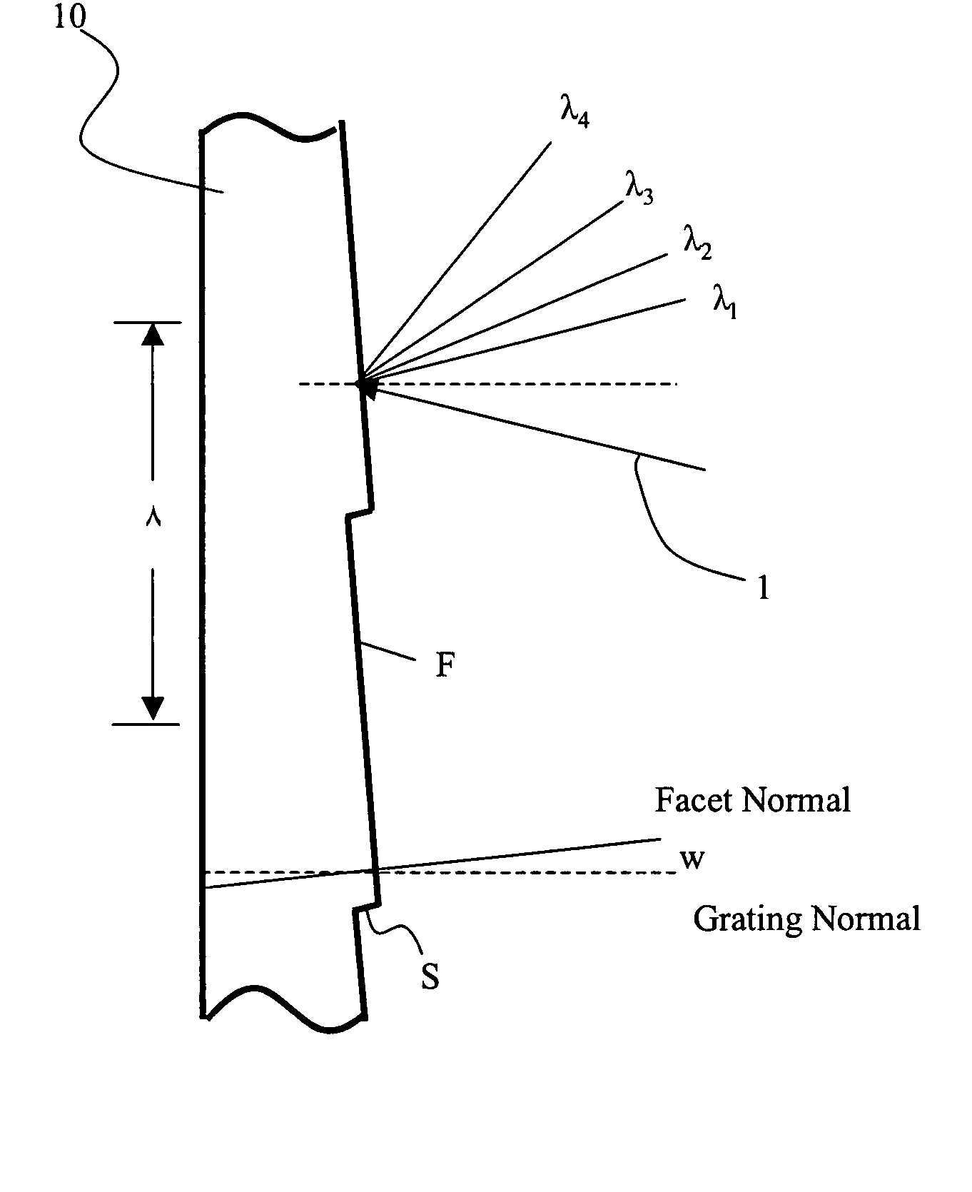
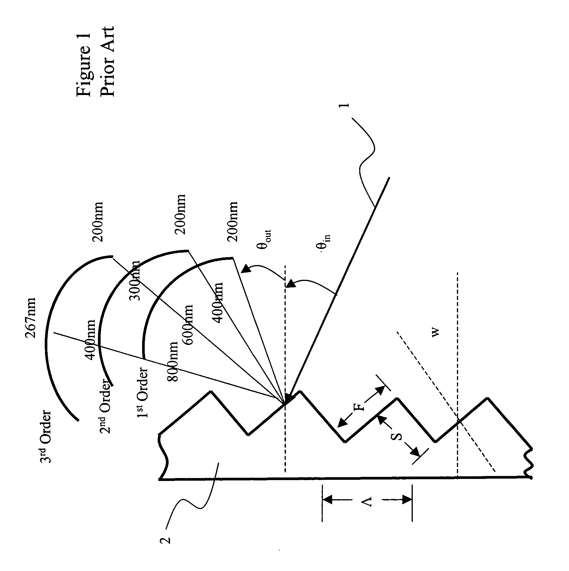
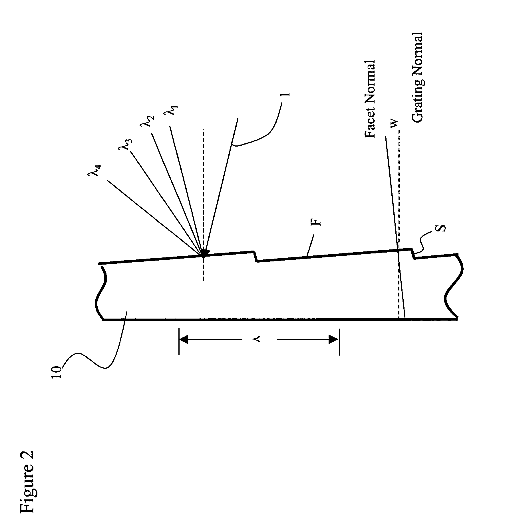
[0045]One of the major concerns in the design of planar waveguide diffraction gratings is the manufacturability of the reflecting and sidewall facets F and S, respectively. Furthermore, a major limit to the manufacturability of the facets heretofore, has been the photolithographic resolution limitations. Typical photolithographic procedures are limited to resolutions in the range of 0.5 to 1.0 μm, so the minimal requirement to achieve reasonable performance from a grating is that the reflecting facet size F must be larger than this resolution, say 2.5 to 5 μm or more in size.

[0046]In FIG. 1, the light path is simplified by the assumption that the input and output angles θin and θNout, respectively are identical. This assumption is only to simplify the mathematical treatment of the facet geometry. Accordingly:

F≈Λ cos θin; and  (6)

[0047]Equation (1) simplifies to

mλ≈2Λ sin θin  (7)

[0048]Combining equations 6 and 7 yields

[0049]F≈m⁢⁢λ2⁢⁢tan⁢⁢θin(8)

[0050]From FIG. 1:

[0051]SF≈tan⁢⁢θin(9)

[0...


PUM


Abstract

The invention relates to a planar waveguide reflective diffraction grating for use in an optical device, such as a wavelength division multiplexer, providing an increased bandwidth over conventional planar waveguide reflection diffraction gratings while eliminating the polarization dependent loss (PDL) typically associated therewith. Accordingly, a low order (<3), high aspect ratio (>10) grating is provided with a very short side wall (less than the wavelength of the optical signal) for use with incident angles of less than 15°.

Description

CROSS-REFERENCE TO RELATED APPLICATIONS[0001]The present invention claims priority from U.S. patent application Ser. No. 60 / 555,697 filed Mar. 24, 2004, which is incorporated herein by reference.TECHNICAL FIELD[0002]The present invention relates to a reflective diffraction grating for use in optical communication, and in particular to a planar waveguide reflective diffraction grating device with reduced polarization sensitivity and an increased free spectral range.BACKGROUND OF THE INVENTION[0003]In optics, a diffraction grating is an array of fine, parallel, equally spaced grooves (“rulings”) on a reflecting or transparent substrate, which grooves result in diffractive and mutual interference effects that concentrate reflected or transmitted electromagnetic energy in discrete directions, called “orders,” or “spectral orders.”[0004]The groove dimensions and spacings are on the order of the wavelength in question. In the optical regime, in which the use of diffraction gratings is mos...

Claims


Application Information

Patent Timeline
Patent Type & Authority Patents(United States)
IPC IPC(8): G02B5/18G02B6/34H04J14/02
CPCG02B6/29326G02B6/29328G02B6/2938G02B6/34H04J14/02
Inventor BIDNYK, SERGEBALAKRISHNAN, ASHOKPEARSON, MATT
Owner ENABLENCE
Why Eureka
Try Eureka