
Flexible macrocell interconnect

a macrocell and interconnection technology, applied in the field of integrated circuits, can solve the problems of large die area consumed by interconnect lines and related routing resources, become more complex, and achieve the effect of improving user-defined function fitting and greater flexibility

Inactive Publication Date: 2007-01-09
ALTERA CORP
View PDF3 Cites 12 Cited by
  • Summary
  • Abstract
  • Description
  • Claims
  • Application Information

AI Technical Summary

Benefits of technology

These structures and methods improve first-time fitting efficiency and provide greater flexibility during second-time fitting, reducing the necessity for hand placement and routing or device upgrades, thereby optimizing resource use and design flexibility.

Problems solved by technology

Programmable logic integrated circuits such as PALs, PLDs, FPGAs, LCAs, and others, are becoming more complex and continually evolving to provide more user-programmable features on a single integrated circuit.
But these programmable interconnect lines and related routing resources consume a large amount of die area.
But keeping the pinout fixed, or “locked,” reduces the flexibility that the fitter has to make changes needed, that is to do a second time fitting.
Often, this means the user has to hand place and route parts of the design, or move to a larger and more expensive device.

Method used


Image

  • Flexible macrocell interconnect
  • Flexible macrocell interconnect
  • Flexible macrocell interconnect

Examples


Embodiment Construction

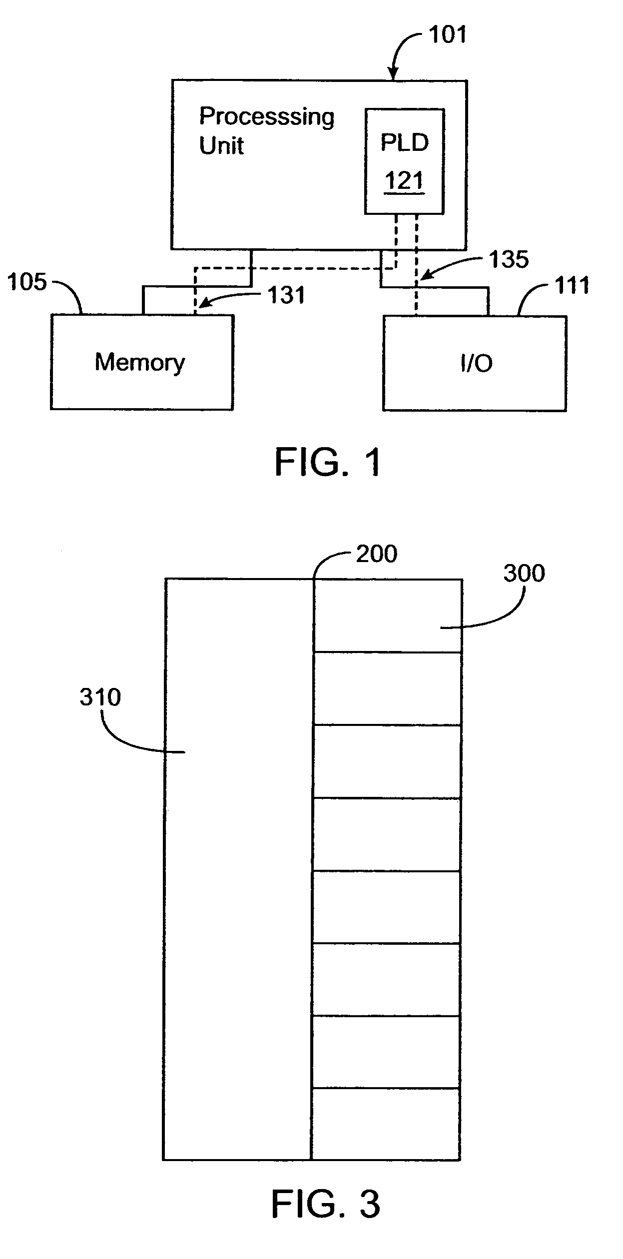
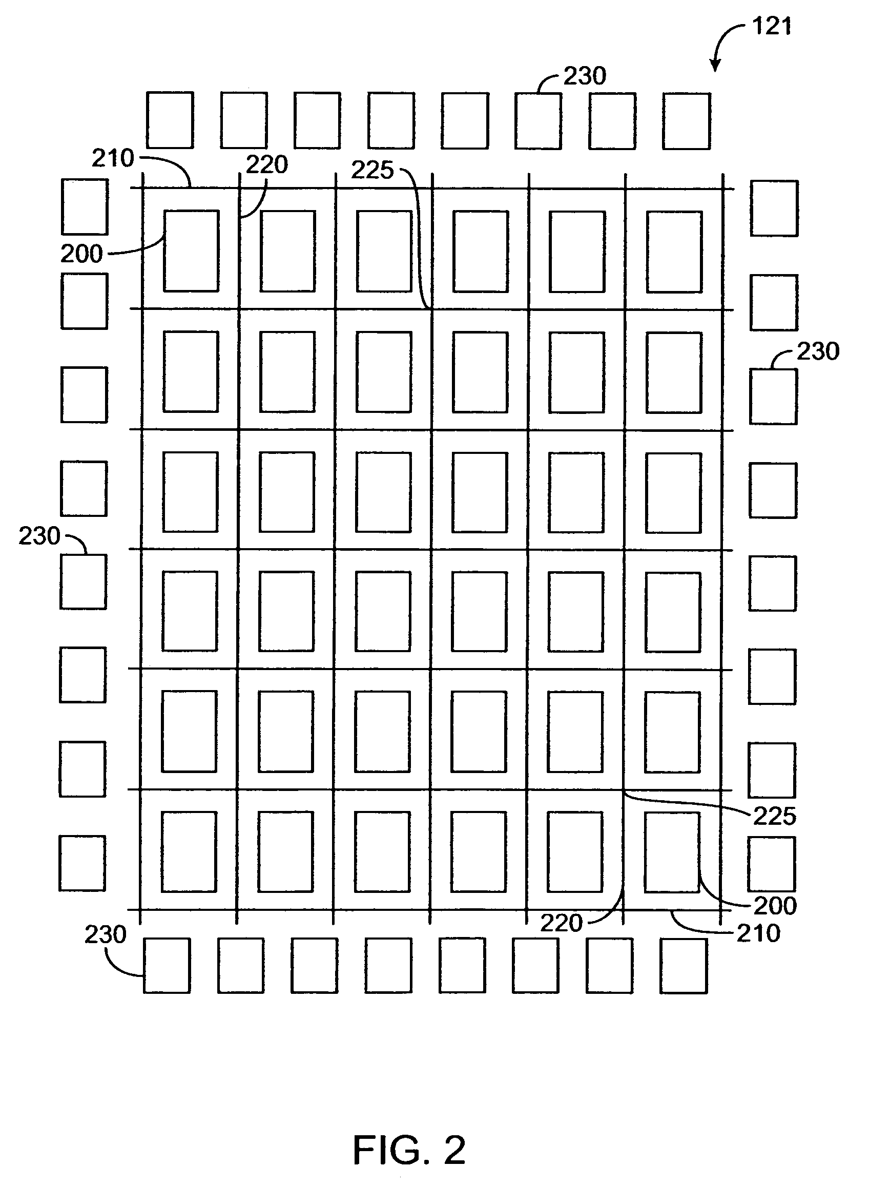
[0035]FIG. 1 shows a block diagram of a digital system, within which the present invention may be embodied. The system may be provided on a single board, on multiple boards, or within multiple enclosures. FIG. 1 illustrates a system 101 in which a programmable logic device 121 may be utilized. Programmable logic devices or programmable logic integrated circuits are sometimes referred to as a PALs, PLAs, FPLAs, PLDs, CPLDs, EPLDs, EEPLDs, LCAs, or FPGAs and are well-known integrated circuits that provide the advantages of fixed integrated circuits with the flexibility of custom integrated circuits. Such devices allow a user to electrically program standard, off-the-shelf logic elements to meet a user's specific needs. Examples of current programmable logic devices are represented by Altera's Classic, MAX®, FLEX®, and APEX™ series of PLDs. These are described in, for example, U.S. Pat. Nos. 4,617,479, 4,871,930, 5,241,224, 5,258,668, 5,260,610, 5,260,611, 5,436,575, and the Altera Dat...


PUM


Abstract

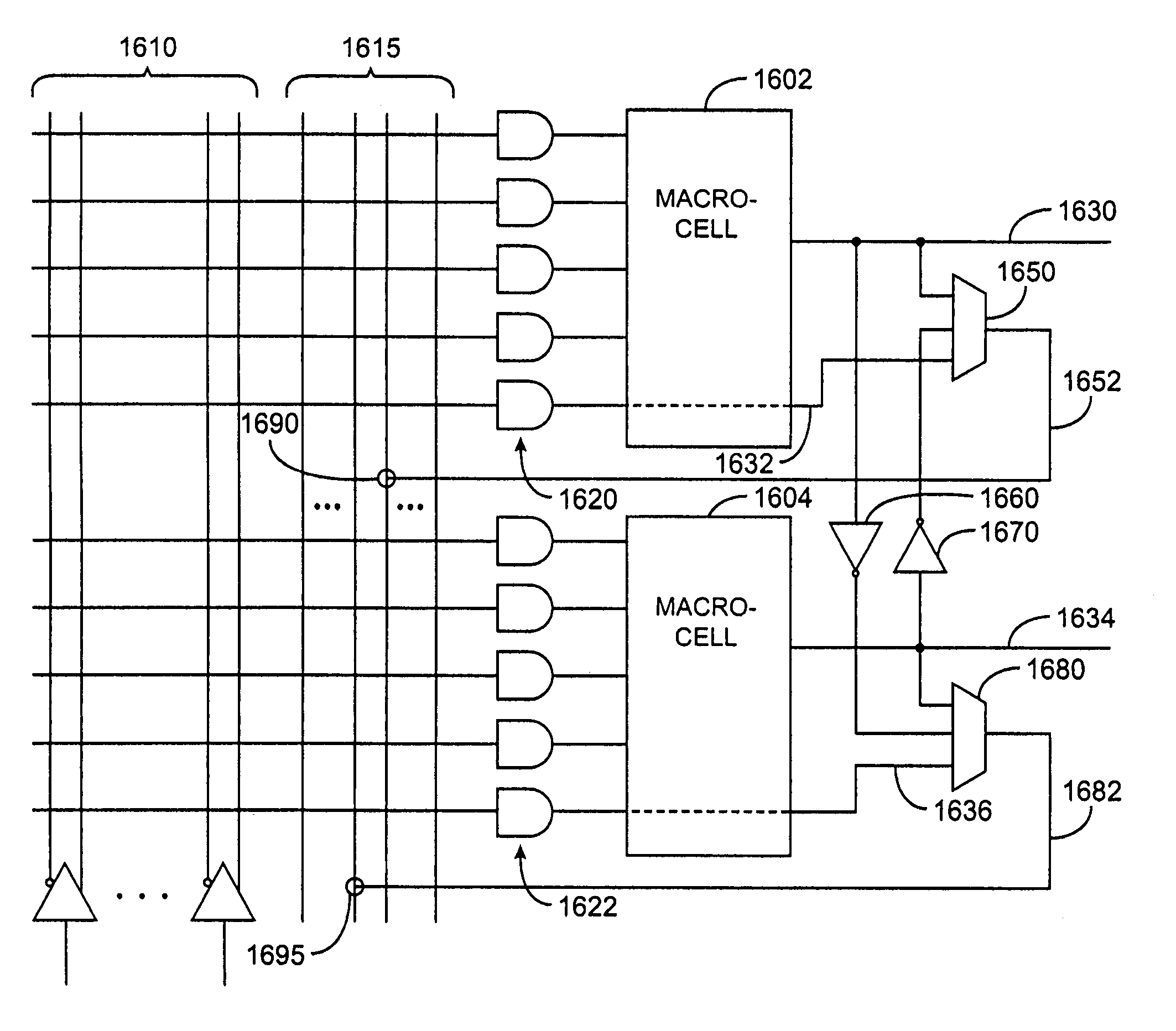
Methods and apparatus for novel routing structures and methods that improve fitting of user-defined functions onto programmable logic devices. In particular, second time fitting is improved. Exemplary structures and methods include allowing product terms to be expanded using inputs from more than one neighboring macrocell by providing multiple expansion and bypassing paths. Also, product term OR shifting prevents macrocell output stages from being buried and made inaccessible, and macrocell outputs are provided on expander word lines, increasing efficiency of those lines, as well as conserving routing resources. Expansion, bypassing, OR shifting, and expander word lines may terminate at logic array block boundaries or may continue beyond these boundaries to other logic array blocks.

Description

[0001]This application is a divisional of U.S. patent application Ser. No. 10 / 301,506, filed Nov. 21, 2002, now U.S. Pat. No. 6,927,601, which is incorporated by reference.BACKGROUND OF THE INVENTION[0002]The present invention relates to the field of integrated circuits, particularly to programmable logic integrated circuits with macrocells having highly flexible interconnect.[0003]Integrated circuits are important building blocks of the modern age. Technology continues to evolve and integrated circuits continue to provide improved functionality. As integrated circuits improve, so do the electronics systems that are built using integrated circuits. There are many types of integrated circuits such as memories, microprocessors, application specific integrated circuits (ASICs), and veprogrammable logic. Programmable logic integrated circuits such as PALs, PLDs, FPGAs, LCAs, and others, are becoming more complex and continually evolving to provide more user-programmable features on a si...

Claims


Application Information

Patent Timeline
Patent Type & Authority Patents(United States)
IPC IPC(8): H03K19/177
CPCH03K19/17736
Inventor LIN, GUUTRAN, STEPHANIEPEDERSON, BRUCEVEST, BRADPARK, JIMSCHLEICHER, JAY
Owner ALTERA CORP
Learn More