Self-boosting system for flash memory cells

a flash memory cell and self-boosting technology, applied in static storage, digital storage, instruments, etc., to achieve the effect of reducing the drain side boosted voltage, reducing leakage, and increasing the channel length

Active Publication Date: 2007-01-09
SANDISK TECH LLC
View PDF38 Cites 122 Cited by
  • Summary
  • Abstract
  • Description
  • Claims
  • Application Information

AI Technical Summary

Benefits of technology

[0020]The undesirable change of charge state can be prevented in multi-level threshold voltage type memories as well as binary-level threshold voltage memories by using appropriate biasing conditions. The application of appropriate biasing conditions may have the effect of causing breakdown mechanism(s) such as band-to-band tunneling at the drain side of the source select transistor to be reduced to such an extent that it does not result in a change of the desired charge storage state of the transistor next to the source select transistor to a different charge state; in some cases, such mechanism(s) may be suppressed completely.
[0030]Another mechanism that can cause program disturb occurs especially at relatively high values of Vpass. In such a case, the drain side area is boosted to a high voltage which can cause breakdown at the drain side of the isolation transistor that is located next to the selected wordline. A possible mechanism of that breakdown is band-to-band tunneling at or close to the edge of the drain area of the isolation memory cell. Other breakdown mechanisms may occur as well. Due to the breakdown, electrons are generated that may become so called “hot electrons” since these electrons can be accelerated by the strong electric field that is present in the neighborhood of the selected wordline. These hot electrons may be injected in the floating gate of the memory cell on the selected wordline or in floating gates of neighboring memory cells, thus changing the threshold voltage of those memory cells and possibly causing a change in the charge storage state of the memory cell. By choosing appropriate biasing voltages for the isolation memory cells, the breakdown at the drain side area of the isolation transistor can be prevented or at least suppressed significantly. Another possible side effect of the breakdown is that the drain side boosted area is partly discharged by the breakdown. Since the breakdown generates hole / electron pairs, electrons flowing to the drain side boosted channel area will lower the boosted potential of that area thereby possibly causing increased program disturb.

Problems solved by technology

This threshold voltage shift may cause the transistor 48 to change from one charge state to another, such as from one programmed state to a different programmed state, which is undesirable.

Method used


Image

  • Self-boosting system for flash memory cells
  • Self-boosting system for flash memory cells
  • Self-boosting system for flash memory cells

Examples


Embodiment Construction

Memory System

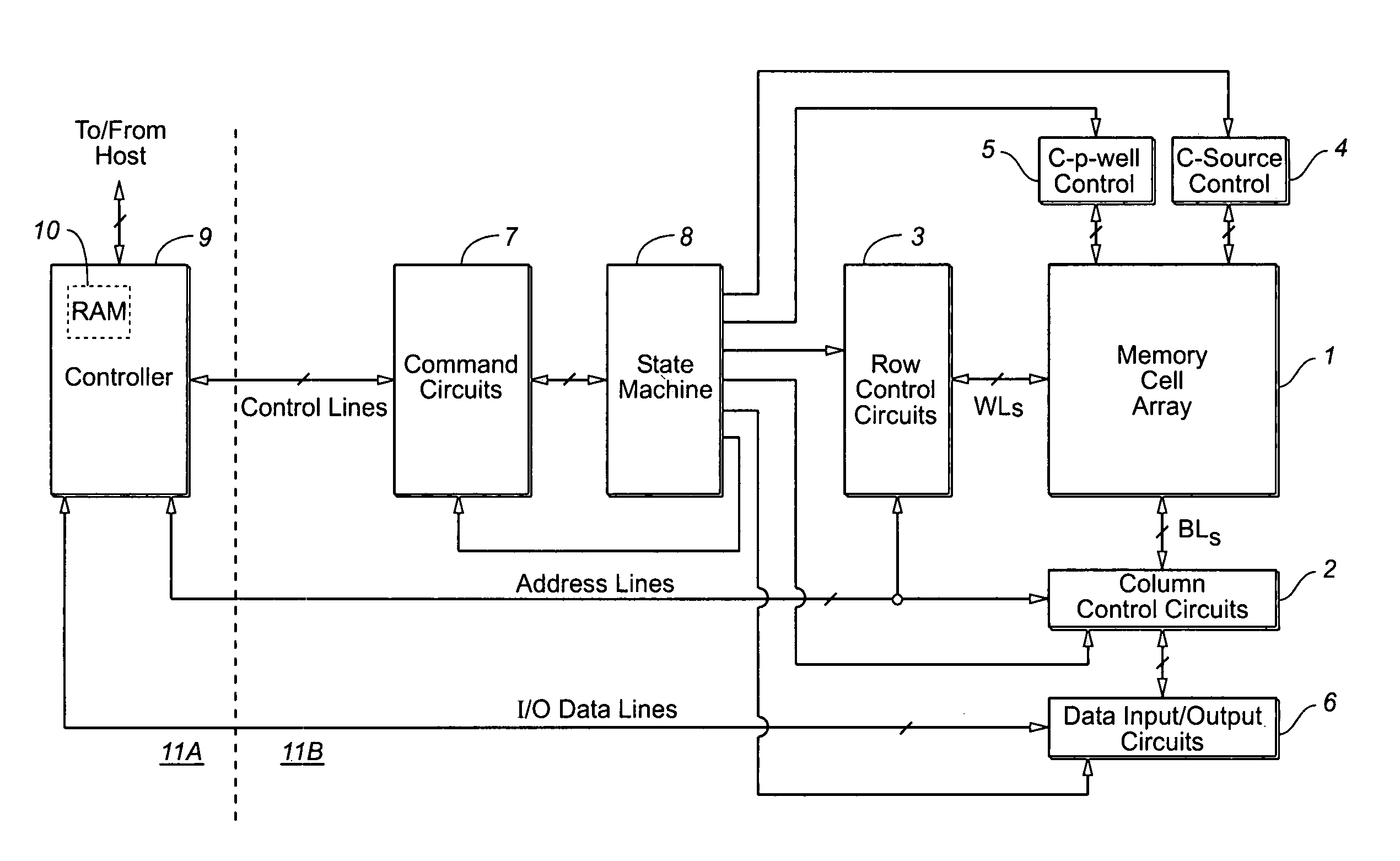
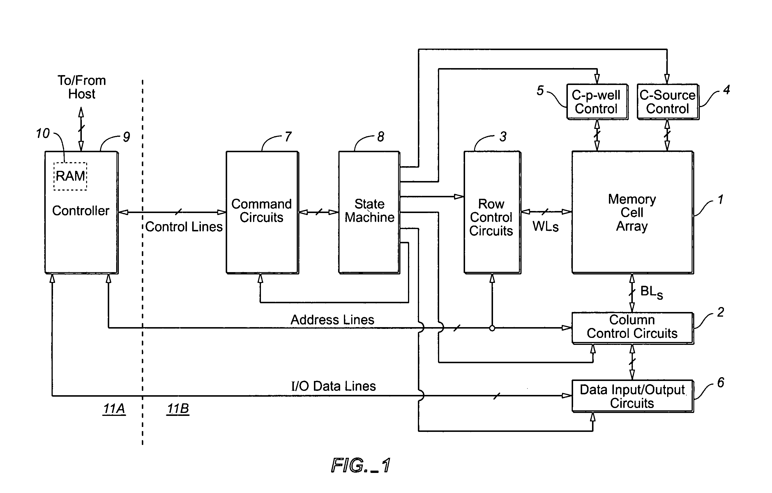
[0043]An example memory system in which the various aspects of the present invention may be implemented is illustrated by the block diagram of FIG. 1. A memory cell array 1 including a plurality of memory cells M arranged in a matrix is controlled by a column control circuit 2, a row control circuit 3, a c-source control circuit 4 and a c-p-well control circuit 5. The memory cell array 1 is, in this example, of the NAND type that is described above in the Background and in references incorporated herein by reference. A control circuit 2 is connected to bit lines (BL) of the memory cell array 1 for reading data stored in the memory cells (M), for determining a state of the memory cells (M) during a program operation, and for controlling potential levels of the bit lines (BL) to promote the programming or to inhibit the programming. The row control Circuit 3 is connected to word lines (WL) to select one of the word lines (WL), to apply read voltages, to apply program volt...


PUM


Abstract

A low voltage of the order of or one to three volts instead of an intermediate VPASS voltage (e.g. of the order of five to ten volts) is applied to word line zero immediately adjacent to the source or drain side select gate of a NAND flash device to reduce or prevent the shifting of threshold voltage of the memory cells coupled to word line zero during the programming cycles of the different cells of the NAND strings. This may be implemented in any one of a variety of different self boosting schemes including erased areas self boosting and local self boosting schemes. In a modified erased area self boosting scheme, low voltages are applied to two or more word lines on the source side of the selected word line to reduce band-to-band tunneling and to improve the isolation between two boosted channel regions. In a modified local self boosting scheme, zero volt or low voltages are applied to two or more word lines on the source side and to two or more word lines on the drain side of the selected word line to reduce band-to-band tunneling and to improve the isolation of the channel areas coupled to the selected word line.

Description

BACKGROUND OF THE INVENTION[0001]This invention relates generally to non-volatile semiconductor memories of the flash EEPROM (Electrically Erasable and Programmable Read Only Memory) type, particularly to structures and methods of operating NAND types of memory cell arrays.[0002]There are many commercially successful non-volatile memory products being used today, particularly in the form of small form factor cards, which use an array of flash EEPROM cells.[0003]One popular flash EEPROM architecture utilizes a NAND array, wherein a large number of strings of memory cells are connected through one or more select transistors between individual bit lines and a reference potential. A portion of such an array is shown in plan view in FIG. 2A. BL0–BL4 (of which BL1–BL3 are also labeled 12–16) represent diffused bit line connections to global vertical metal bit lines (not shown). Although four floating gate memory cells are shown in each string, the individual strings typically include 16, ...

Claims


Application Information

Patent Timeline
Patent Type & Authority Patents(United States)
IPC IPC(8): G11C11/34G11C11/56G11C16/04G11C16/10
CPCG11C16/10G11C16/0483G11C16/30G11C16/04
Inventor HEMINK, GERRIT JAN
Owner SANDISK TECH LLC
Why Eureka
Try Eureka