Digital pixel sensor with clock count output and operating method thereof

a digital pixel sensor and clock count technology, applied in the field of pixels, can solve problems such as increasing costs, and achieve the effect of increasing the dynamic rang

Active Publication Date: 2007-01-16
VIA TECH INC
View PDF6 Cites 50 Cited by
  • Summary
  • Abstract
  • Description
  • Claims
  • Application Information

AI Technical Summary

Problems solved by technology

The digital pixel sensor, however, includes a large number of transistors, and therefore increases costs.

Method used


Image

  • Digital pixel sensor with clock count output and operating method thereof
  • Digital pixel sensor with clock count output and operating method thereof
  • Digital pixel sensor with clock count output and operating method thereof

Examples


Embodiment Construction

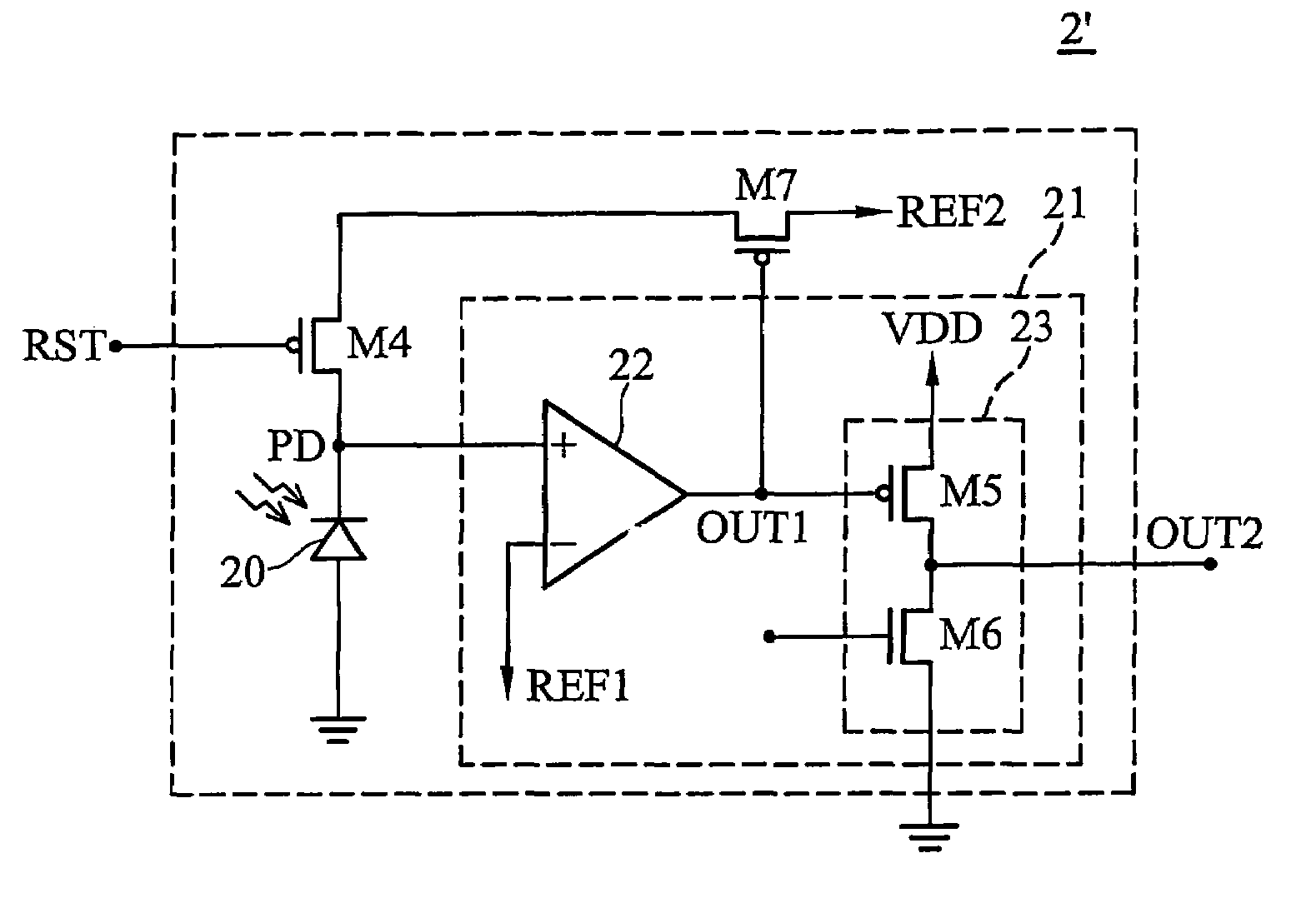
[0025]FIG. 5 is a schematic diagram of a digital pixel sensor (DPS) in accordance with the present invention. The digital pixel sensor 2 includes a first switch M4, a light sensing unit 20, and a decision device 21.

[0026]The first switch M4 is connected between a node PD and a specific voltage source, and its gate receives a reset signal RST turning it on or off. Here the first switch M4 can be a PMOS or a NMOS transistor, wherein if a PMOS transistor is employed, the Reset level of the node PD does not depend on the threshold voltage of the first switch M4. Additionally, the specific voltage source in the embodiment is realized by a voltage source VDD, although the disclosure is not limited thereto.

[0027]The light sensing unit 20, such as a photodiode or phototransistor, is coupled to the node PD. When the first switch turns off, the light sensing unit 20 detects incident light from an incident light source and generate a photocurrent or transformation current in response. The volt...


PUM


Abstract

A digital pixel sensor, comprising a first switch coupled between a first voltage and a first node, turned on or off by a rest signal to provide a first voltage to the first node when turned on; a light sensing unit coupled to the first node generating a transformation current responsive to the intensity of an incident light source and thereby discharging the first node, and a decision device coupled with the first node and a reference signal to output an intensity reference signal corresponding to the intensity of the incident light source when the voltage at the first node is discharged to a level below that of the reference signal.

Description

CROSS-REFERENCE TO RELATED APPLICATION[0001]This application claims priority to U.S. provisional application Ser. No. 60 / 577,260, filed Jun. 4, 2004.BACKGROUND[0002]The invention relates to a pixel sensor and more particularly to a digital pixel sensor (DPS) employing MOS transistors.[0003]FIG. 1 is a circuit diagram illustrating a conventional analog pixel sensor. As shown in FIG. 1, the analog pixel sensor 1 includes a photodiode 10, a MOS transistor M1, a MOS transistor M2, and a MOS transistor M3.[0004]When operating, the voltage of a reset signal RS is first pulled up to a high level, turning on transistor M1 and pulling the voltage at node PD up to VDD-Vth, where Vth is the threshold voltage of the transistor M1. Reset signal RS is then pulled down to a low level, turning off the transistor M1 and allowing the voltage of node PD to float. Photo diode 10 is illuminated by an incident light source, which produces a photocurrent of electron-hole pairs to flow in the photo diode 1...

Claims


Application Information

Patent Timeline
Patent Type & Authority Patents(United States)
IPC IPC(8): H03K17/78H03M1/12H01L27/00H03K5/153H03K17/94H04L27/148H04N5/335
CPCH03K17/941H03K2217/94106H04N25/772
Inventor LAI, CHENG-HSIAOKING, YA-CHIN
Owner VIA TECH INC
Why Eureka
Try Eureka