
Eureka
For R&D, Eureka makes reading and utilizing patents & technical documents easy.
Eureka AIR
Designed for self-driven R&D workflows. Generate viable solutions, solve complex R&D challenges, empower your innovation with AI.

Eureka Materials
Designed for material experts only. Revolutionize your material R&D, from search, analyze, to developing new materials.

TechResearch
Generate reliable direction feasibility study reports for your R&D in just a few steps.

TechSeek
Discover and master advanced knowledge NOW. Basics, ideas, possibilities, all at once.

TechMind
As an expert in R&D Theories, TechMind can generates customized viable solutions instantly.

TechRisk
Analyze your overall solution with one click, know your potential R&D risks in advance.

TechMonitor
Get weekly tech updates, stay abreast of the latest tech innovations and key insights.
Semiconductor device and method for forming same using multi-layered hard mask
- Summary
- Abstract
- Description
- Claims
- Application Information
AI Technical Summary
Benefits of technology
Problems solved by technology
Method used
Image

Examples
Embodiment Construction
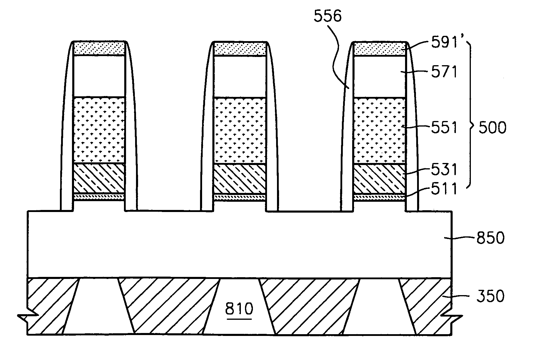
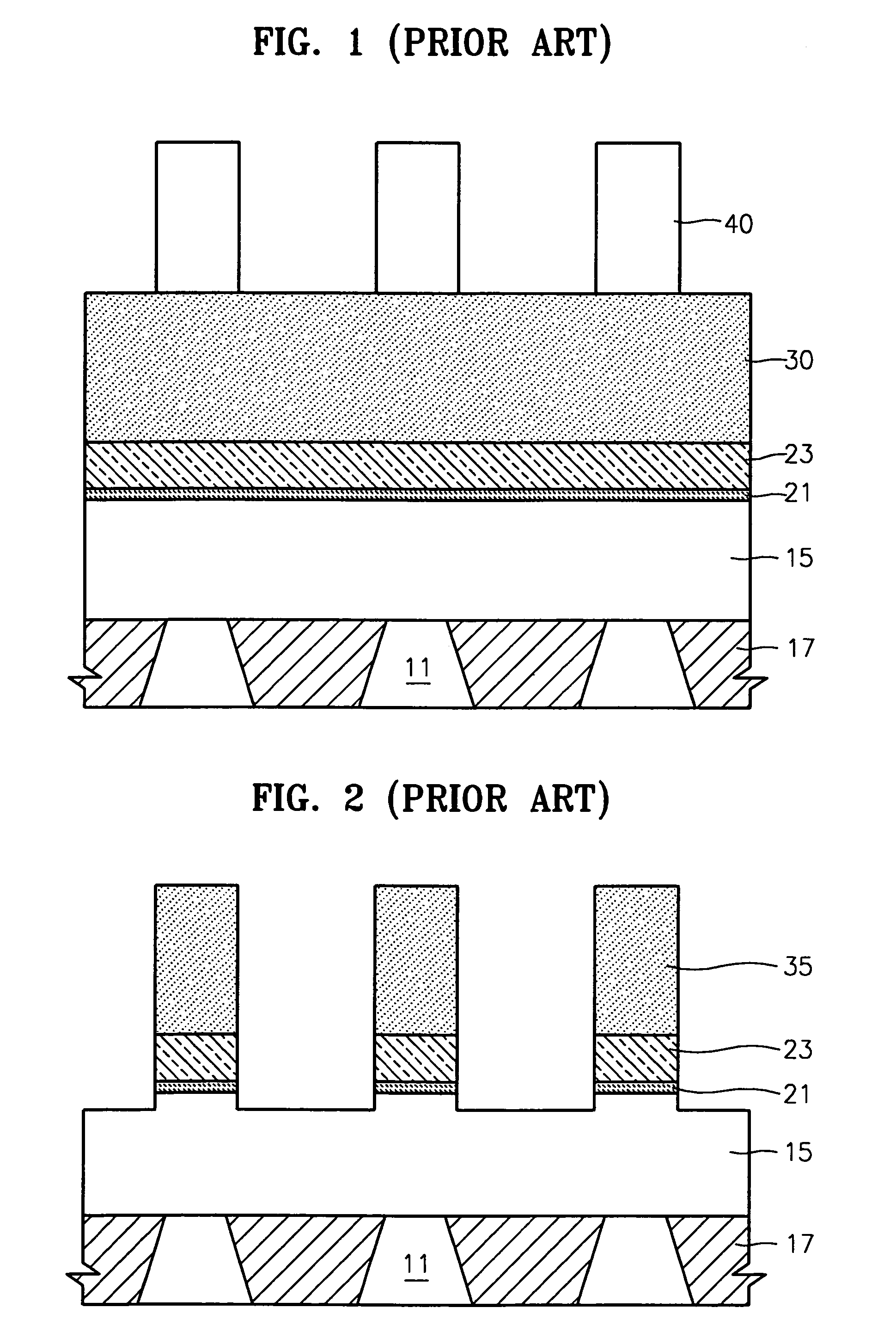
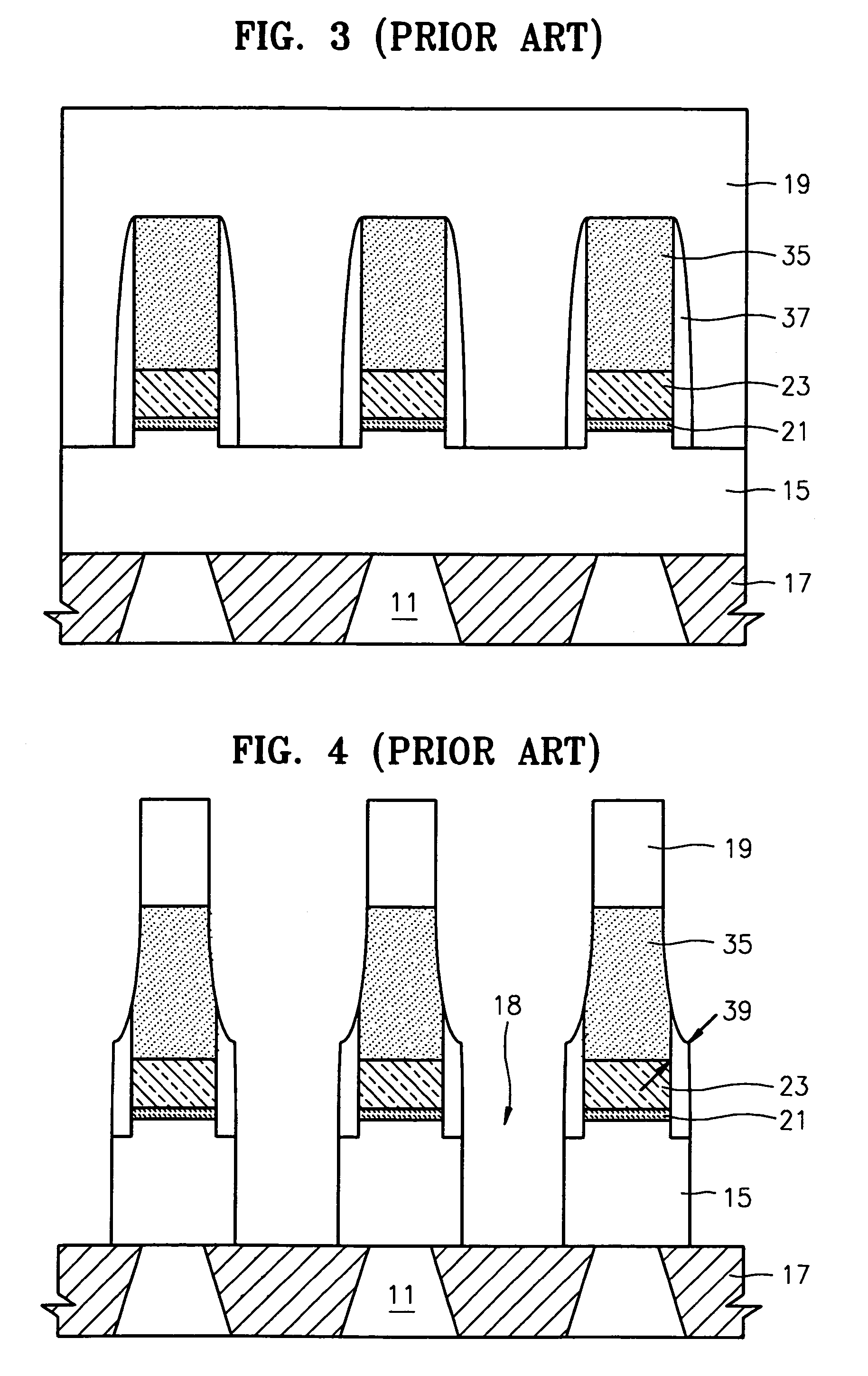
[0022]In embodiments of the invention, as in COB-type DRAM devices, interconnecting contacts such as capacitor contacts are formed between wire lines such as bit lines. Here, a multi-layered hard mask is used when the bit lines are patterned in order to secure sufficient insulating margins or shoulder margins between the bit lines and the interconnecting contacts. Also, after the bit lines are patterned, while contact holes are being formed to be aligned with the patterned bit lines and penetrate an interlayer dielectric, some layers constituting the multi-layered hard mask can be protected from damage caused by an etching process. Thus, even if the contact holes are formed, the hard mask can remain on the bit lines to a required thickness or more. As a result, sufficient insulating margins can be secured between the capacitor contacts (i.e., BCs) for filling the contact holes and the bit lines. Also, spacers formed for protecting the sidewalls of the bit lines can be formed of sili...
PUM
 Abstract
Description
Claims
Application Information
 - R&D Engineer
- R&D Manager
- IP Professional
- Industry Leading Data Capabilities
- Powerful AI technology
- Patent DNA Extraction
Browse by: Latest US Patents, China's latest patents, Technical Efficacy Thesaurus, Application Domain, Technology Topic, Popular Technical Reports.
© 2024 PatSnap. All rights reserved.Legal|Privacy policy|Modern Slavery Act Transparency Statement|Sitemap|About US| Contact US: help@patsnap.com