Eureka AIR delivers breakthrough ideas for toughest innovation challenges, trusted by R&D personnel around the world.

Method for fabricating semiconductor device

Inactive Publication Date: 2007-09-13
PROMOS TECH INC
View PDF13 Cites 11 Cited by
  • Summary
  • Abstract
  • Description
  • Claims
  • Application Information

AI Technical Summary

Benefits of technology

[0010] Another object of the present invention is to provide a method for fabricating a semiconductor device adapted for lowering parasitic capacitance caused by a bit-line coupling effect.
[0014] The above-mentioned methods are adapted for lowering parasitic capacitances in IC structures by forming an opening within the spacer formed along a sidewall of the semiconductor device. The methods also employ selective epitaxial process to grow an epitaxial silicon layer and form an air gap so that the parasitic capacitances caused by a bit-line coupling effect may be further lowered.

Problems solved by technology

While integrated circuits (IC) become denser to a certain degree, e.g., micrometer scale, the surface area of such a semiconductor chip is far from enough for allowing required interconnects set up.
Unfortunately, there is often an unwanted so-called parasitic capacitance occurred between a double-layer conductive structure having a dielectric layer sandwiched therebetween, i.e., a conductor / dielectric / conductor layer stacked structure.
Such a parasitic capacitance often raises a signal noise that affects the workability and even the reliability of the device.

Method used


Image

  • Method for fabricating semiconductor device
  • Method for fabricating semiconductor device
  • Method for fabricating semiconductor device

Examples


Embodiment Construction

[0020] Reference will now be made in detail to the present preferred embodiments of the invention, examples of which are illustrated in the accompanying drawings. Wherever possible, the same reference numbers are used in the drawings and the description to refer to the same or like parts.

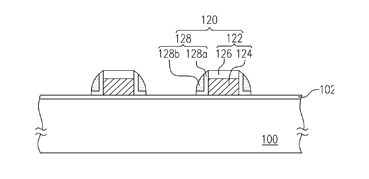
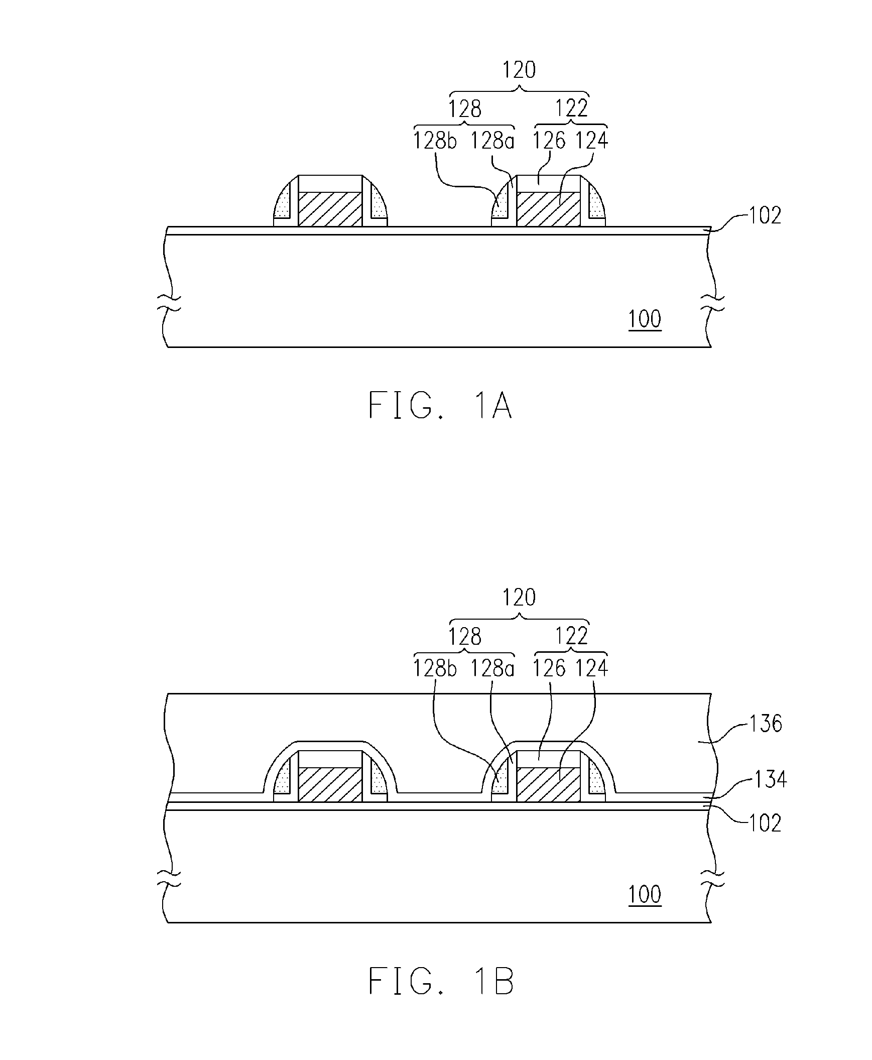
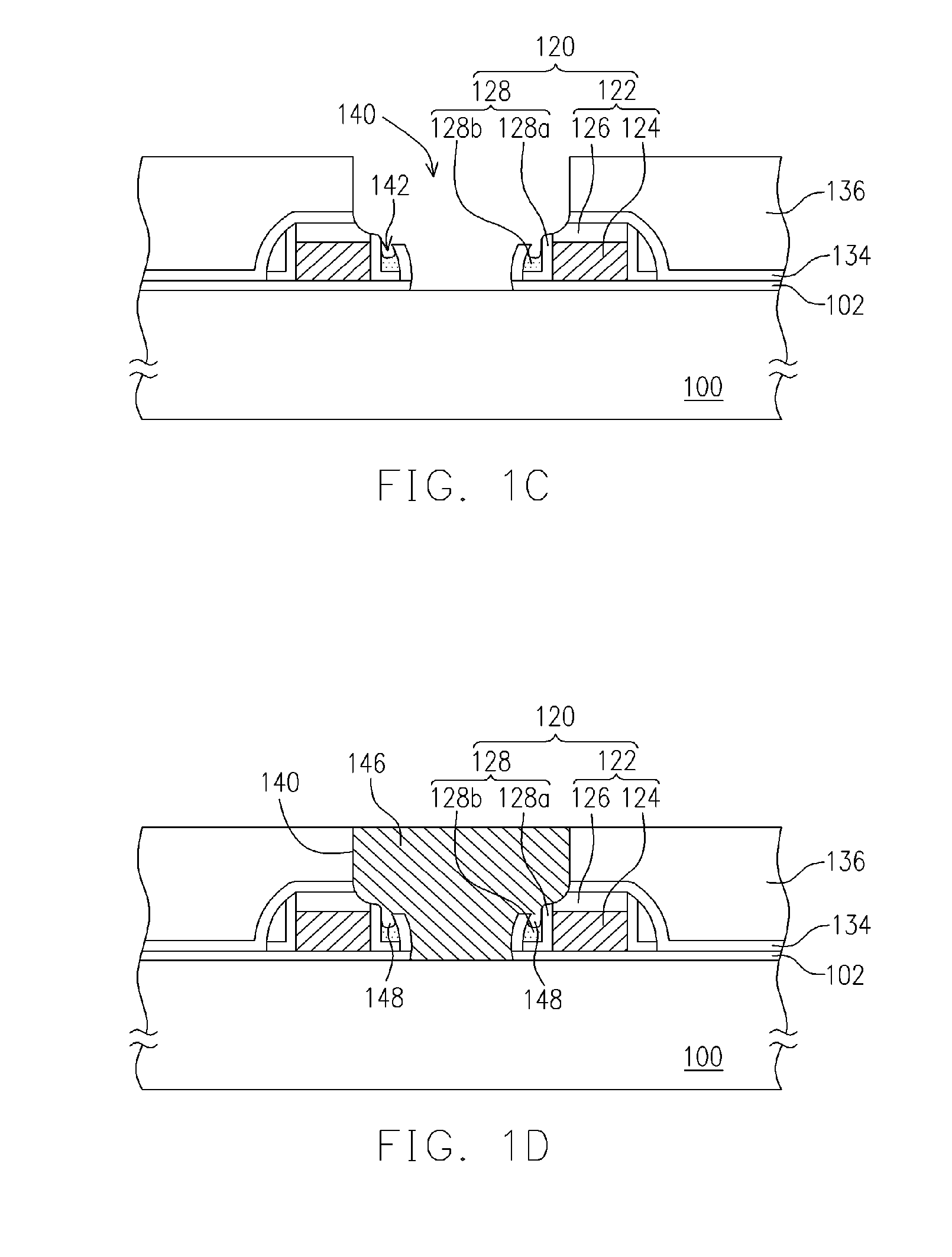
[0021]FIGS. 1A to 1D are cross-sectional views illustrating a method for fabricating a semiconductor device according to an embodiment of the present invention. This embodiment is exemplified with a memory cell device. However the present invention is not limited thereto, other semiconductor devices, e.g., metallic-oxide semiconductor (MOS) devices may also be adapted purpose of the present invention.

[0022] Referring to FIG. 1A, a thin oxide layer is formed on a substrate 100. The oxide layer serves as a gate dielectric layer 102. The gate dielectric layer 102 is, for example, made of silicon oxide, and may be formed by, for example, a thermal oxidization method or a chemical vapor deposition (CVD...


PUM


Abstract

A method for fabricating a semiconductor device is described. A gate dielectric layer is formed on a substrate. A plurality of gate structures are formed on the gate dielectric layer. Each of the gate structures is composed of a stacked structure and a spacer. Each stacked structure includes a gate conductive layer and a cap layer. The spacer includes a first dielectric layer and a second dielectric layer. A barrier layer is formed over the substrate covering conformally the gate structures and the gate dielectric layer. A dielectric layer is formed on the barrier layer. A self-aligned contact window etching process is conducted to form a contact window opening. A SEG process is conducted to grow an epitaxial silicon layer to form a contact window and an air gap in the opening.

Description

CROSS-REFERENCE TO RELATED APPLICATION [0001] This application claims the priority benefit of Taiwan application serial no. 95108076, filed on Mar. 10, 2006. All disclosure of the Taiwan application is incorporated herein by reference. BACKGROUND OF THE INVENTION [0002] 1. Field of the Invention [0003] The present invention relates to a method for fabricating a semiconductor device, and particularly to a method for fabricating a semiconductor device that is adapted for lowering parasitic capacitance thereof. [0004] 2. Description of Related Art [0005] Along with the development of semiconductor technology, the sizes of the semiconductor devices have become smaller and smaller. While integrated circuits (IC) become denser to a certain degree, e.g., micrometer scale, the surface area of such a semiconductor chip is far from enough for allowing required interconnects set up. An approach addressing thereto for a very large scale integration (VLSI) is employing multi-layer metallic inter...

Claims


Application Information

Patent Timeline
IPC IPC(8): H01L21/336
CPCH01L21/28525H01L21/76897H01L21/76879H01L21/7682
Inventor CHUNG, CHAO-HSIKUO, WEN-SHUO
Owner PROMOS TECH INC
Why Eureka
Eureka Blog
Learn More