Method for fabricating semiconductor device and semiconductor device
a semiconductor and semiconductor technology, applied in the direction of coatings, transistors, chemical vapor deposition coatings, etc., can solve the problems of inability to achieve excellent electric characteristics of capacitors, inability to reduce the size of memory cells, and uneven thickness of ferroelectric films obtained, etc., to achieve excellent electric characteristics
- Summary
- Abstract
- Description
- Claims
- Application Information
AI Technical Summary
Benefits of technology
Problems solved by technology
Method used
Image

Examples
first embodiment
[0064](First Embodiment)
[0065]Hereinafter, a method for fabricating a semiconductor device according to a first embodiment of the present invention will be described with reference to FIG. 1.
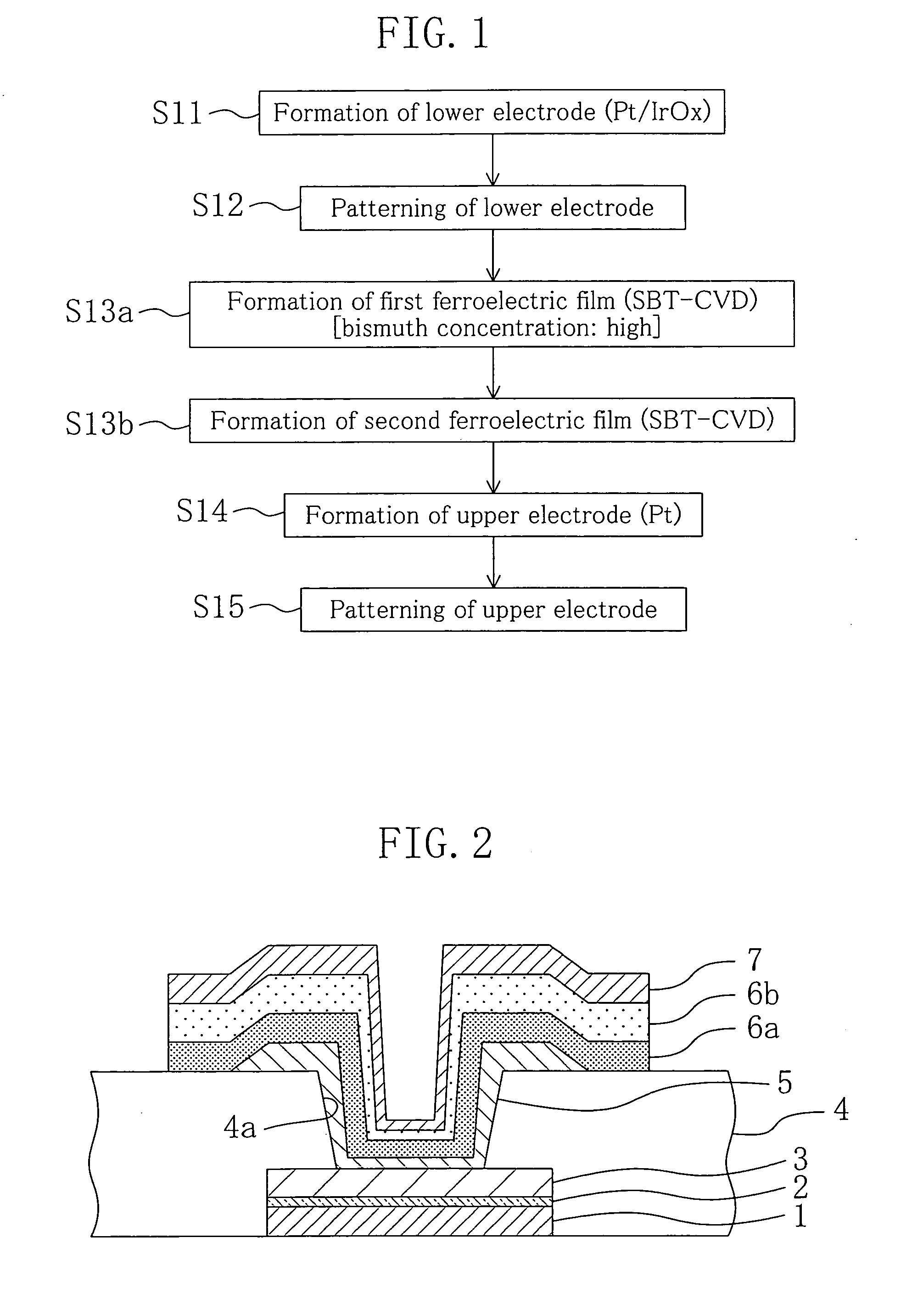
[0066]FIG. 1 is a flow chart showing a method for fabricating a semiconductor device according to the first embodiment of the present invention.
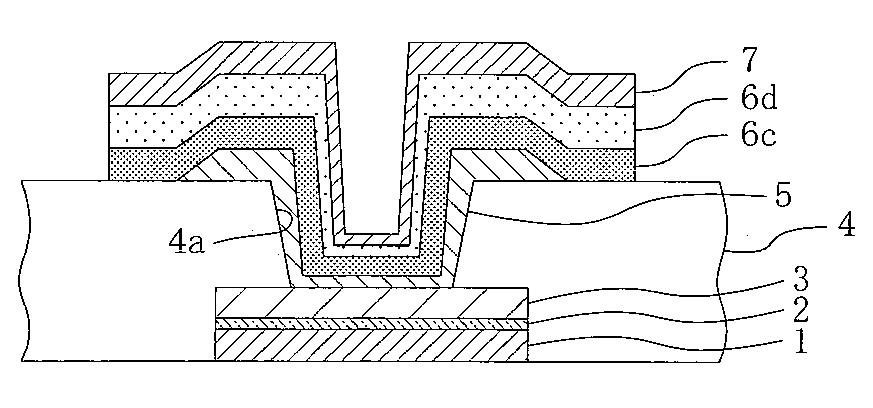
[0067]A lamination film of indium oxide, iridium and titanium aluminum nitride is formed on a semiconductor substrate in advance, and then a silicon oxide film is formed over the semiconductor substrate so as to cover the lamination film. Furthermore, a recess portion is formed in the silicon oxide film so that part of a surface of the lamination film is exposed through the recess portion (not shown).
[0068]Next, in Step S11, a lower electrode formed of a platinum (Pt) film is formed along inner surfaces of the recess portion in the silicon oxide film by sputtering. Note that the lower electrode may be formed of a lamination film of platinum (Pt) and irid...
second embodiment
[0095](Second Embodiment)
[0096]Hereinafter, a method for fabricating a semiconductor device according to a second embodiment of the present invention will be described with reference to FIG. 6.
[0097]FIG. 6 is a flow chart showing a method for fabricating a semiconductor device of the second embodiment of the present invention.
[0098]A lamination film of indium oxide, iridium and titanium aluminum nitride is formed on a semiconductor substrate in advance, and then a silicon oxide film is formed over the semiconductor substrate so as to cover the lamination film. Furthermore, a recess portion is formed in the silicon oxide film so that part of a surface of the lamination film is exposed through the recess portion (not shown).
[0099]Next, in Step S21, a lower electrode formed of a platinum (Pt) film is formed along inner surfaces of the recess portion in the silicon oxide film by sputtering. Note that the lower electrode may be formed of a lamination film of platinum (Pt) and iridium oxi...
third embodiment
[0125](Third Embodiment)
[0126]Hereinafter, a third embodiment of the present invention will be described with reference to FIG. 11.
[0127]FIG. 11 is a flow chart showing a method for fabricating a semiconductor device according to the third embodiment of the present invention.
[0128]A lamination film of indium oxide, iridium and titanium aluminum nitride is formed on a semiconductor substrate in advance, and then a silicon oxide film is formed over the semiconductor substrate so as to cover the lamination film. Furthermore, a recess portion is formed in the silicon oxide film so that part of a surface of the lamination film is exposed through the recess portion (not shown).
[0129]Next, in Step S31, a lower electrode formed of a platinum (Pt) film is formed along inner surfaces of the recess portion in the silicon oxide film by sputtering. Note that the lower electrode may be formed of a lamination film of platinum (Pt) and iridium oxide (IrOx).
[0130]Next, in Step S32, the lower electro...
PUM
| Property | Measurement | Unit |
|---|---|---|
| flow rate | aaaaa | aaaaa |
| flow rate | aaaaa | aaaaa |
| flow rate | aaaaa | aaaaa |
Abstract
Description
Claims
Application Information
 - R&D Engineer
- R&D Manager
- IP Professional
- Industry Leading Data Capabilities
- Powerful AI technology
- Patent DNA Extraction
Browse by: Latest US Patents, China's latest patents, Technical Efficacy Thesaurus, Application Domain, Technology Topic.
© 2024 PatSnap. All rights reserved.Legal|Privacy policy|Modern Slavery Act Transparency Statement|Sitemap