Solid-state imaging device and imaging apparatus

a solid-state imaging and imaging device technology, applied in the field of solid-state imaging devices and imaging apparatuses, can solve the problems of sudden fluctuations in the power supply voltage, the driving load placed on the circuit driving various control lines, and the above-mentioned problems, so as to achieve non-uniform circuit configuration

Active Publication Date: 2011-08-04
SONY SEMICON SOLUTIONS CORP
View PDF4 Cites 10 Cited by
  • Summary
  • Abstract
  • Description
  • Claims
  • Application Information

AI Technical Summary

Benefits of technology

[0015]The embodiments of the invention makes it possible to provide a solid-state imaging device and an imaging apparatus in which electric charges can be prevented from flowing from an optical black pixel region into

Problems solved by technology

Problems as described below have occurred in CMOS type solid-state imaging devices having a dummy pixel region provided between an effective pixel region and an optical black pixel region.
First, since the dummy pixel region is always kept in an unselected state, when signals are read out from each row of pixels of the pixel array section, driving loads placed on circuits driving vario

Method used


Image

  • Solid-state imaging device and imaging apparatus
  • Solid-state imaging device and imaging apparatus
  • Solid-state imaging device and imaging apparatus

Examples


Embodiment Construction

[0035]Hereinafter, embodiments of the invention will now be described. The description is made in the order listed below.

[0036]1. Configuration of Imaging Apparatus

[0037]2. Configuration of Solid-State Imaging device

[1. Configuration of Imaging Apparatus]

[0038]A configuration of an imaging apparatus according to an embodiment of the invention will now be described with reference to the drawings.

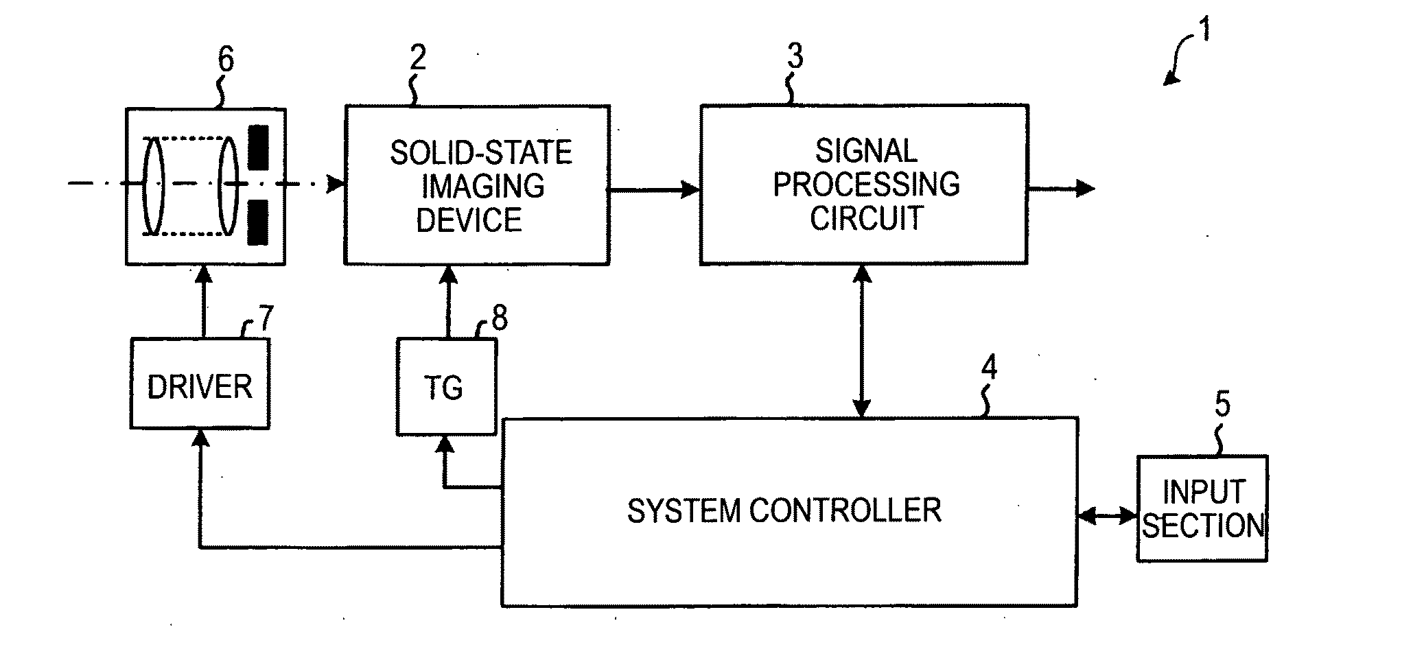
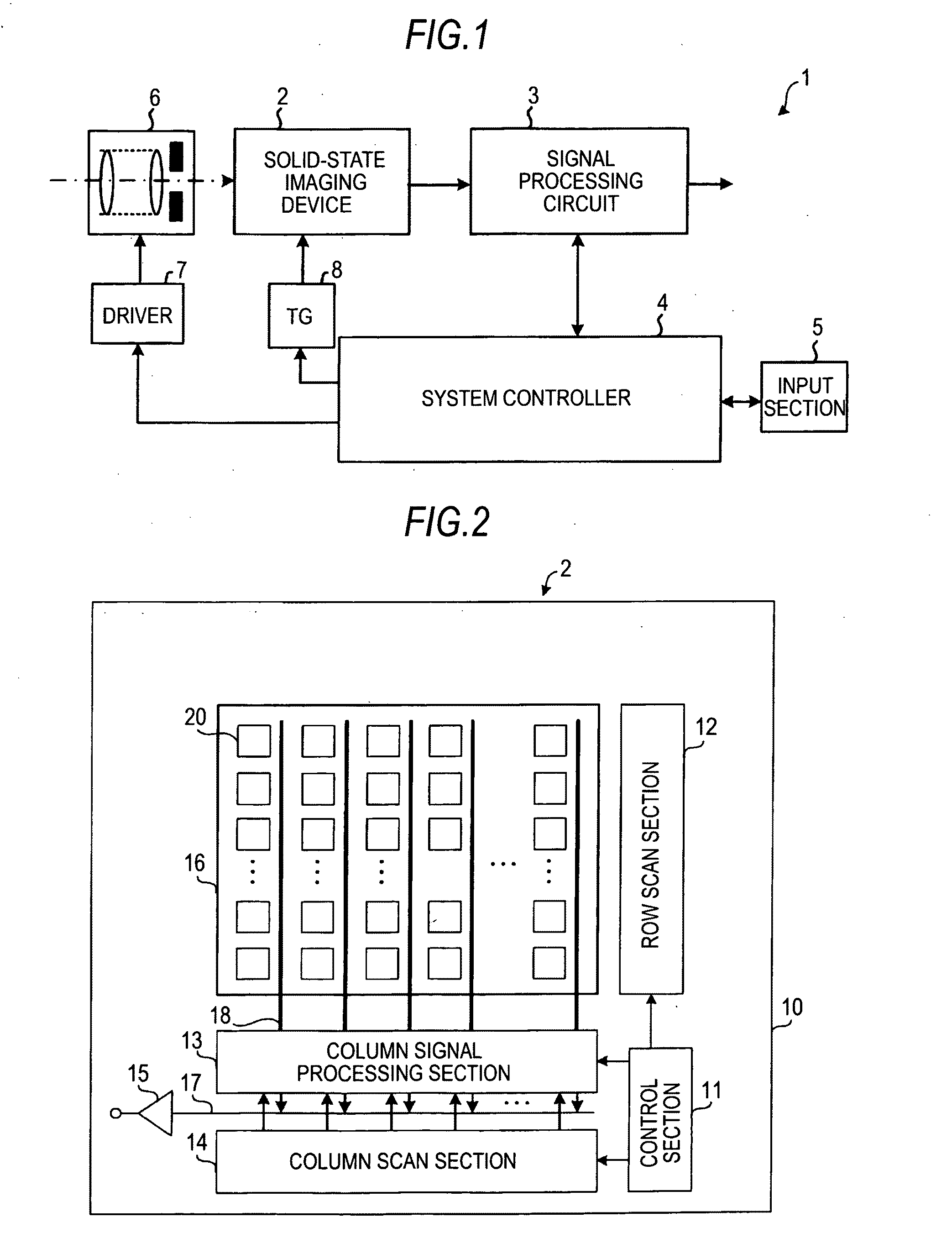
[0039]As shown in FIG. 1, an imaging apparatus 1 includes a solid-state imaging device 2, a signal processing circuit 3, a system controller 4, an input section 5, and an optical block 6. The imaging apparatus 1 also includes a driver 7 for driving mechanisms in the optical block 6 and a timing generator (TG) for driving the solid-state imaging device 2. The solid-state imaging device 2 is a CMOS type solid-state imaging device.

[0040]The optical block 6 includes a lens for converging light from an object on the solid-state imaging device 2, a driving mechanism for moving the lens for focusing...


PUM


Abstract

A solid-state imaging device includes: a pixel array section having an effective pixel region formed by a plurality of pixels which are disposed in the form of a matrix, each of which includes a photoelectric conversion device and a transistor reading out an electric charge obtained by photoelectric conversion at the photoelectric conversion device, and which are illuminated by light and a light-shielded pixel region formed by a plurality of pixels which are shielded from light; a row scan section selecting and controlling each row of pixels of the pixel array section to output a signal from each of the pixels of the selected row of pixels to a column signal line provided in association with the row of pixels; and an A-D conversion section converting the signal output from the signal line into a digital signal.

Description

BACKGROUND OF THE INVENTION[0001]1. Field of the Invention[0002]The present invention relates to a CMOS type solid-state imaging device and an imaging apparatus having such an element.[0003]2. Description of the Related Art[0004]Recently, imaging apparatus capable of imaging utilizing a solid-state imaging device and capable of storing resultant images have widely spread, such apparatus including digital still cameras and digital video cameras. CCD type solid-state imaging devices have been most commonly used as solid-state imaging devices of such imaging apparatus. However, there is a recent trend toward solid-state imaging devices having a greater number of pixels, as a result of which increasing attention is paid to CMOS type solid-state imaging devices.[0005]A CMOS type solid-state imaging device is a solid-state imaging device which includes a pixel array section constituted by a two-dimensional array of a plurality of pixels each including a photoelectric conversion device and...

Claims


Application Information

Patent Timeline
IPC IPC(8): H04N5/335
CPCH04N5/357H04N5/335H04N25/00H01L27/14623H01L27/14603H01L27/14609H04N25/60
Inventor NIKAI, NORIHIRO
Owner SONY SEMICON SOLUTIONS CORP
Why Eureka
Try Eureka