Printed circuit wiring board designing support device, printed circuit board designing method, and its program

a printed circuit wiring board and supporting device technology, applied in the direction of cad circuit design, program control, instruments, etc., can solve the problems of ic and lsi malfunction generation, high levels of unnecessary electromagnetic wave radiation, and difficulty in realizing such mounting structure of capacitors, so as to promote the optimization of the layout of the board

Active Publication Date: 2007-01-23
NEC CORP
View PDF6 Cites 22 Cited by
  • Summary
  • Abstract
  • Description
  • Claims
  • Application Information

AI Technical Summary

Benefits of technology

[0012]It is an object of the present invention to provide printed circuit board design supporting technology for automatically checking the arrangement of a capacitor for controlling unnecessary electromagnetic wave radiation and circuit malfunction to promote the optimization of a board layout, while maintaining a design approach and the structure of a conventional board.
[0013]More specifically, it is an object of the present invention to provide a printed circuit wiring board design supporting device for automatically checking the arrangement of the capacitor for controlling the unnecessary electromagnetic wave radiation and the circuit malfunction to promote the optimization of the board layout, while maintaining the design approach and the structure of the conventional board.
[0014]It is another object of the, present invention to provide a printed circuit board design method for automatically checking the arrangement of a capacitor for controlling unnecessary electromagnetic wave radiation and circuit malfunction to promote the optimization of a board layout, while maintaining a design approach and the structure of a conventional board.

Problems solved by technology

A multilayer printed circuit board includes a power line composed of aground wiring for providing reference potential of power supply wiring and a circuit for supplying a direct-current voltage required for the IC and the LSI to operate and the potential variation of the power line at high frequency often triggers the generation of IC and LSI malfunction, and high levels of unnecessary electromagnetic wave radiation.
However, with the progress of high-density implementation, a case in which an LSI package and the like requiring high-density wiring called BGA (Ball Grid Array) is increased, leading to difficulty in realizing such mounting structure of the capacitors as shown in FIG. 1A, FIG. 1B, FIG. 2A, FIG. 2B, and FIG. 2C.
Additionally, in a case in which a capacitor is automatically added, it is impossible to determine whether or not the structure is best suited because the relationship between the position at which the capacitor is mounted and unnecessary electromagnetic wave radiation control or circuit malfunction prevention is not clearly defined.

Method used


Image

  • Printed circuit wiring board designing support device, printed circuit board designing method, and its program
  • Printed circuit wiring board designing support device, printed circuit board designing method, and its program
  • Printed circuit wiring board designing support device, printed circuit board designing method, and its program

Examples


first embodiment

(First Embodiment)

[0079]A first embodiment of the present invention will be described below. FIG. 5 is a block diagram showing the configuration of a printed circuit wiring board design supporting device in accordance with the first embodiment of the present invention.

[0080]Referring to FIG. 5, this printed circuit board design supporting device comprises a control part 1 operating under the control of CPU (not shown), an input / output part 2 provided with a key input part and a display part, and an external storage device 3 for storing a database described later.

[0081]The control part 1 includes a layout data input part 11, a plane structure extraction part 12, a via hole extraction part 13, a capacitor extraction part 14, a distance measurement part 15, a database 3, a distance comparison part 16, and a warning generation part 17.

[0082]The layout data input part 11 inputs, layout data of a printed circuit board indicating each arrangement position for the case of mounting the struc...

second embodiment

(Second Embodiment)

[0165]Next, a second embodiment of the present invention will be described.

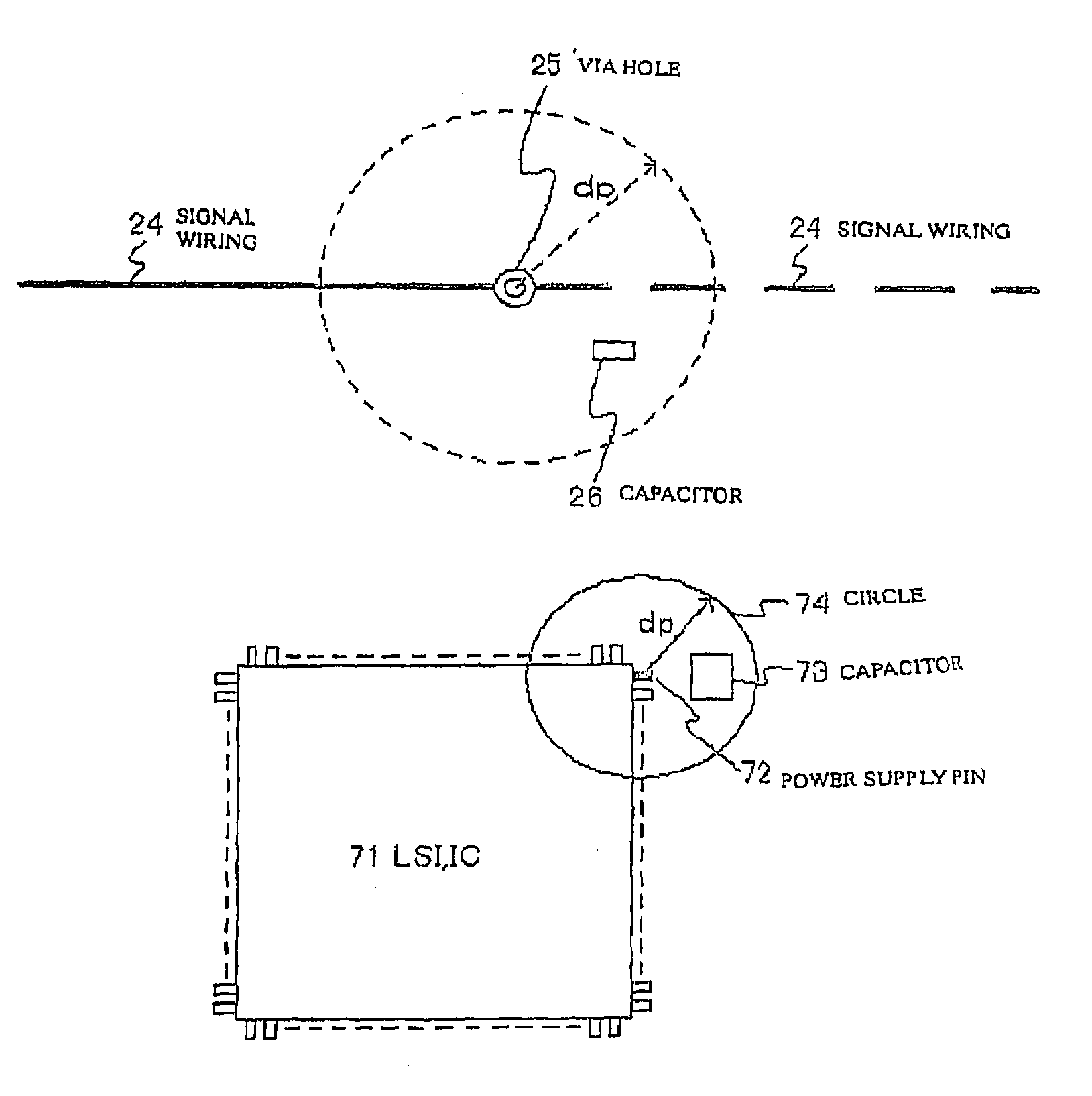
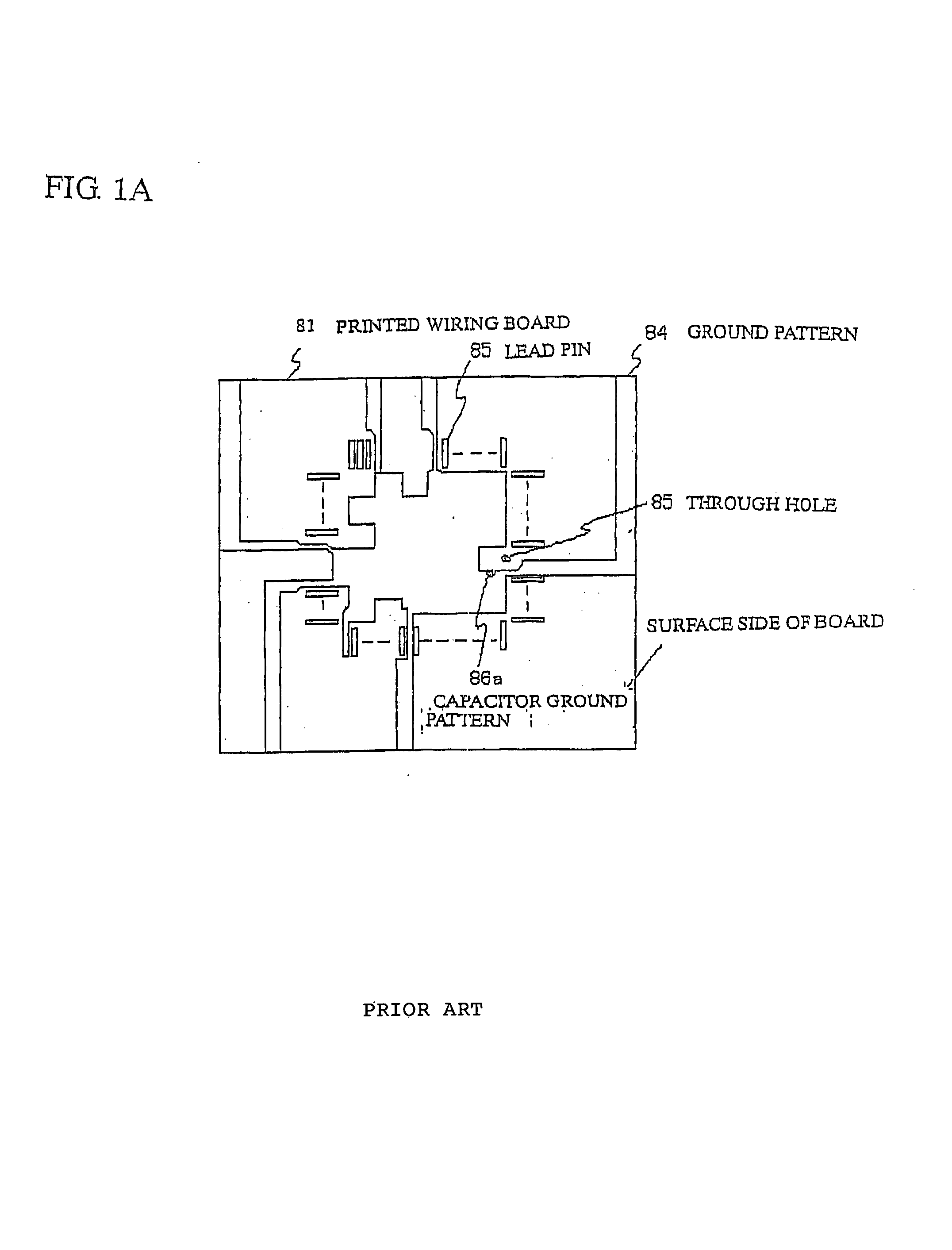
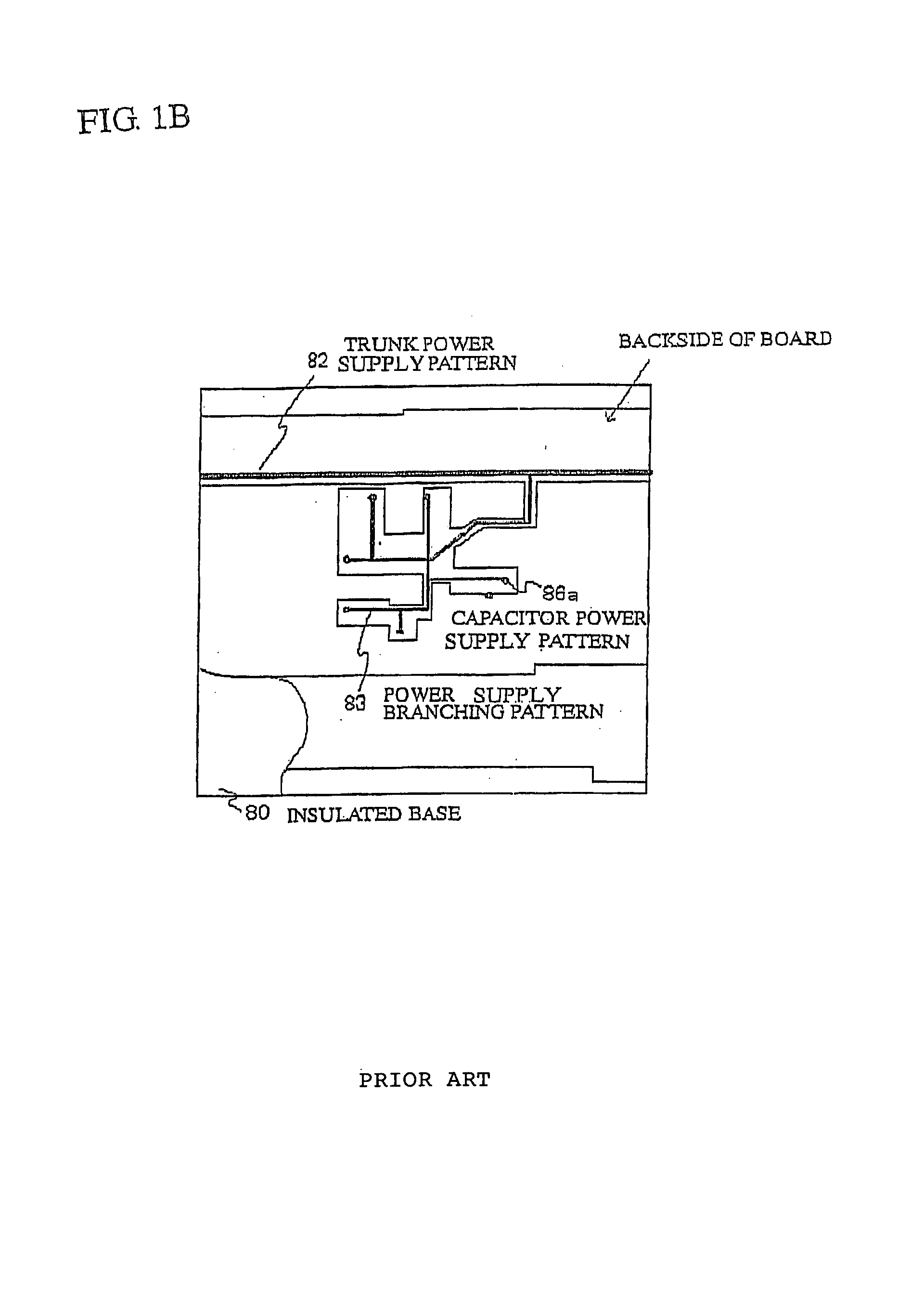
[0166]FIG. 16 is a block diagram showing the configuration of a printed circuit wiring board design supporting device in accordance with the second embodiment of the present invention. FIG. 17 is a flowchart showing a printed circuit wiring board design method in accordance with a printed circuit wiring board design supporting device having the configuration of FIG. 16. FIG. 18A is a partial longitudinal sectional view of a four-layer printed circuit board having a via hole and a capacitor for connecting between different levels of wiring in accordance with the second embodiment of the present invention. FIG. 18B is a diagram showing the relationship between LSI, the power source pin, and the capacitor in FIG. 18A. FIG. 18C is an equivalent circuit diagram of the power plane, the ground plane, the LSI, and the capacitor of the printed circuit board in FIG. 18A.

[0167]This printed circuit wir...


PUM


Abstract

A printed circuit wiring board designing support device includes a layout data receiving section receiving printed circuit board layout data through an input / output section, a section for extracting structures of power supply / ground planes, a via hole extracting section for extracting a via hole interconnecting the wirings extending over power supply / ground planes, a capacitor extracting section for extracting a capacitor connected between power supply / ground planes, a distance measuring section for measuring the distance between the via hole and the capacitor, a database where the allowable distance value between the via hole and the capacitor in respect to the distance between the power supply and ground planes is recorded, an examination section for comparing the capacitor / via hole distance with the allowable distance value, and a warning section for issuing a warning when the distance between the via hole and the capacitor is larger than the allowable distance value.

Description

TECHNICAL FIELD[0001]The present invention relates to a printed circuit wiring board design supporting device, a printed circuit board design method, and a program of the same, and in particular to a printed circuit wiring board design supporting device, a printed circuit board design method, and a program of the same, in which engineering practice for optimizing the arrangement of a bypass capacitor for controlling circuit malfunction due to unnecessary electromagnetic radiation and noise is improved.BACKGROUND ART[0002]For the purpose of more adequately describing a technological level for the present invention at present, all descriptions of the patents, patent applications) patent gazettes, scientific papers, and the like which are cited or specified in tho present application will be incorporated herein by reference.[0003]A printed circuit board comprises electronic components such as IC and LSI, and signal wiring for connecting those components, and is mounted on an almost eve...

Claims


Application Information

Patent Timeline
Patent Type & Authority Patents(United States)
IPC IPC(8): G06F17/50H05K1/02H05K3/00
CPCG06F17/5068H05K3/0005H05K2201/09309H05K1/0231G06F30/39
Inventor HARADA, TAKASHIYAGUCHI, TAKAHIROWAKUI, AKIRAEYA, SEISHIFUJIMOTO, SHUNSUKE
Owner NEC CORP
Why Eureka
Try Eureka