Vertical type semiconductor device

a semiconductor device, vertical type technology, applied in the direction of semiconductor devices, electrical devices, transistors, etc., can solve the problem of not being able to study the effect of structure in a substantial way

Active Publication Date: 2007-01-30
DENSO CORP
View PDF10 Cites 43 Cited by
  • Summary
  • Abstract
  • Description
  • Claims
  • Application Information

AI Technical Summary

Benefits of technology

[0015]Thus, it is possible that the width of the depletion layer spreading from the inside of the column region (4) toward the terminal end (16) of the column region spreads to be equivalent to the width of the depletion layer spreading from the inside of the column region in the depth direction of the substrate. Thus, the electric field is prevented from concentrating at a specific part in a region facing the narrow side of the column structure. The breakdown voltage of the vertical type semiconductor device (i.e., the vertical type MOSFET) is improved.
[0018]The above structures described in the other embodiments of the present invention enables to expand the depletion layer spreading toward the terminal end (16) of the column region to be equivalent to the depletion layer spreading from the inside of the column region (4) in the depth direction of the substrate. Since the electric field is prevented from concentrating at a specific part in a region facing the narrow side of the column structure, the breakdown voltage of the vertical type semiconductor device (i.e., the vertical type MOSFET) is improved.

Problems solved by technology

However, it has not studied substantially about an effective structure of a structure corresponding to the IB—IB cross section shown in FIG. 2B.

Method used


Image

  • Vertical type semiconductor device
  • Vertical type semiconductor device
  • Vertical type semiconductor device

Examples


first embodiment

[0034](First Embodiment)

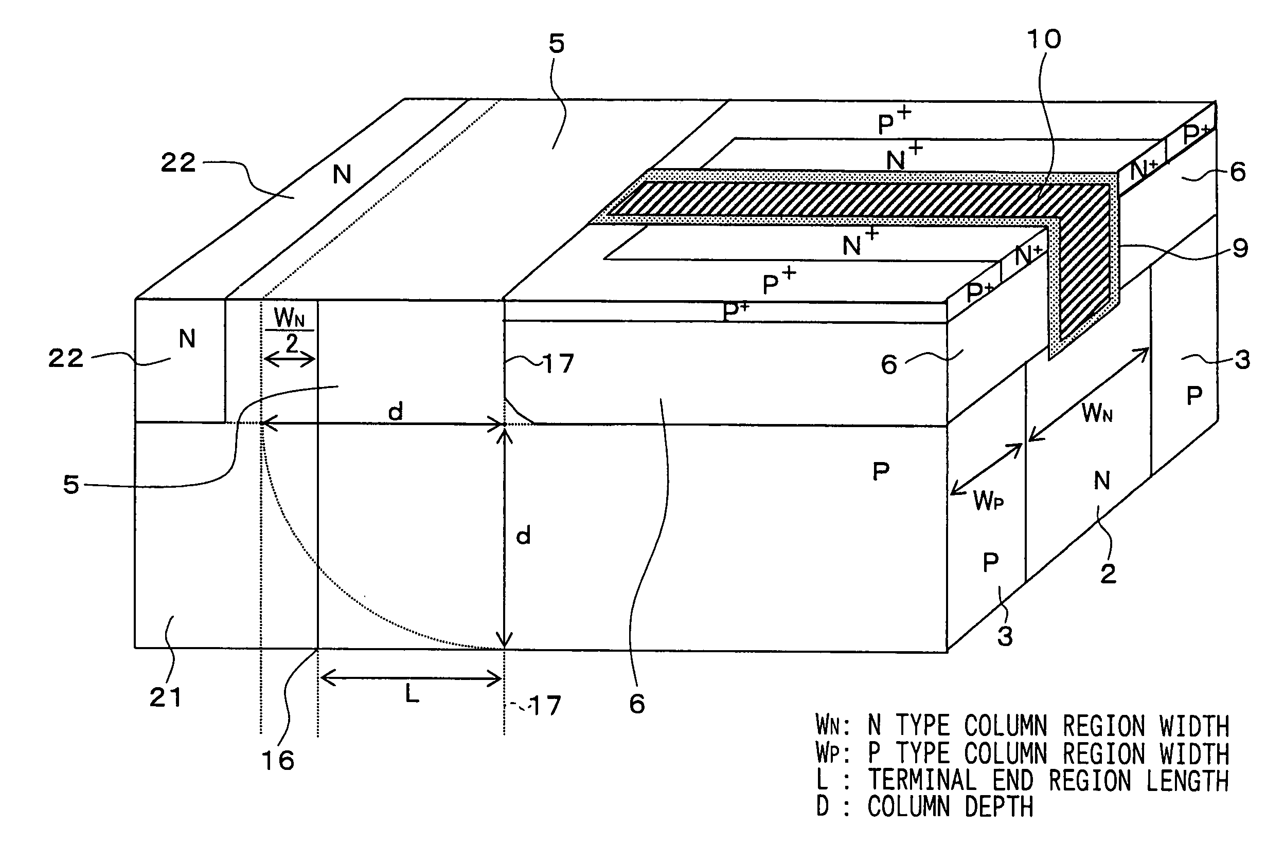
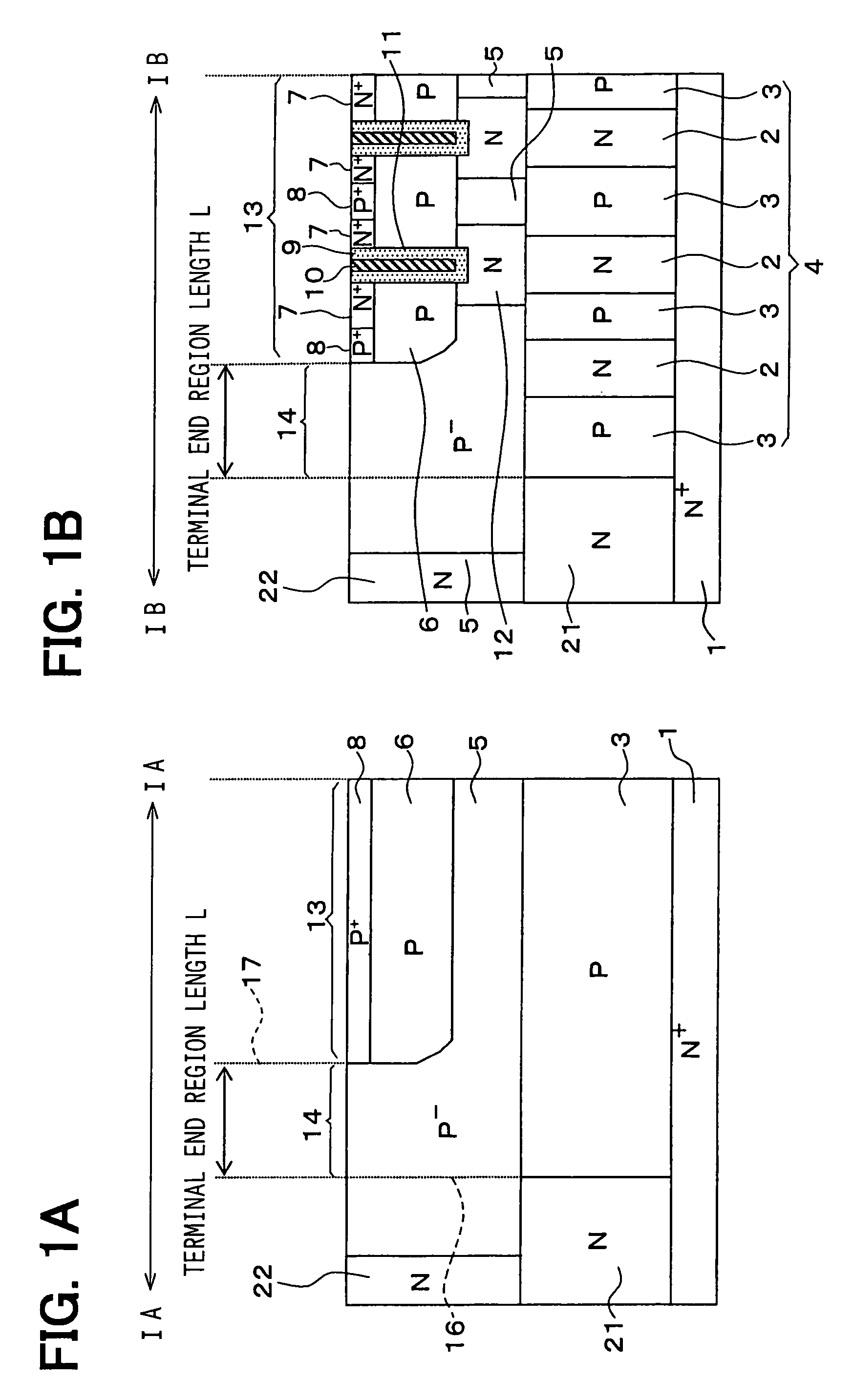
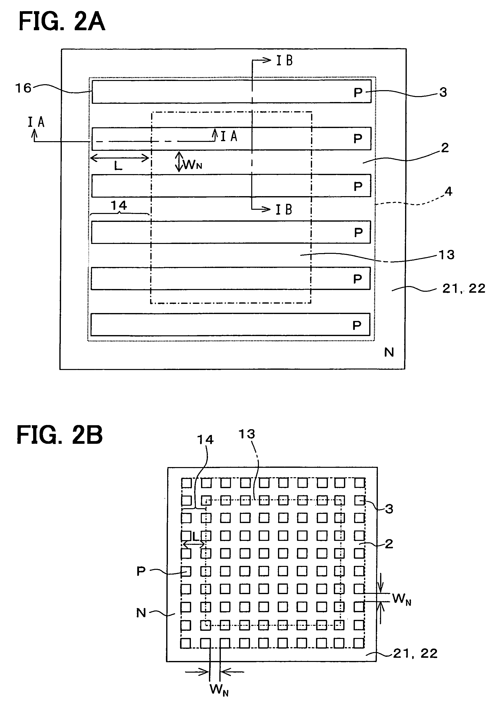
[0035]FIGS. 1A and 1B are cross sectional views showing a vertical type MOSFET according to a first embodiment of the present invention. FIG. 1A shows a structure corresponding to a IA—IA cross sectional view facing a narrow side of a P conductive type column region 3 shown in FIG. 2. To understand this embodiment easily, FIG. 1B shows a structure corresponding to a IB—IB cross sectional view facing a wide side of the P conductive type column region 3 shown in FIG. 2. This structure is known conventionally.

[0036]The vertical type MOSFET shown in the above drawings is explained. The vertical type MOSFET is formed on a semiconductor substrate having a N+ conductive type. The MOSFET includes a N+ conductive type drain region 1, a column region 4, a N+ conductive type source region 7, a P conductive type body region 6, a P+ conductive type body contact region 8 and a trench gate 11.

[0037]The N+ conductive type drain region 1 is formed from the N+ conductive type ...

second embodiment

[0052](Second Embodiment)

[0053]FIG. 6A is a cross sectional view showing a vertical type MOSFT according to a second embodiment of the present invention. This embodiment is different from the first embodiment, the difference such that no P− conductive type semiconductor single crystal region 5 and no N conductive type buffer region 12 in the cross sectional drawing in FIGS. 1A and 1B is disposed on the substrate surface so that the column structure reaches the substrate surface, which includes no P body region 6.

[0054]The layout on the substrate surface corresponds to the IA—IA cross sectional structure facing the narrow side of the P conductive type column region 3, that is similar to the first embodiment. Here, FIG. 6B is described to understand this embodiment easily. FIG. 6B shows a structure corresponding to the IB—IB cross sectional structure facing the wide side of the P conductive column region 3 shown in FIG. 2A, the structure which is well-known conventionally.

[0055]In the...

third embodiment

[0057](Third Embodiment)

[0058]FIG. 7A is a cross sectional view showing a vertical type MOSFET according to a third embodiment of the present invention. FIG. 7A shows a structure corresponding to the VIIA—VIIA cross sectional structure, which faces the narrow side of the P conductive type column region 3 shown in FIG. 8. Here, FIG. 7B is described to understand this embodiment easily. FIG. 7B shows a structure corresponding to the VIIB—VIIB cross sectional structure facing the wide side of the P conductive column region 3 shown in FIG. 8, the structure which is well-known conventionally.

[0059]In the third embodiment, similar to the first embodiment, when the column structure is formed, a Si substrate having a (110)-surface is used. The column structure is formed by a wet-etching method utilizing a surface orientation dependency of an etching rate. Therefore, the shape of the column is different from that in the above described embodiments. The other fundamental structures are simila...


PUM


Abstract

In a vertical type MOSFET device having a super junction structure, in which a N conductive type column region and a P conductive type column region are alternately aligned, regarding to a distance between a terminal end of an active region and a terminal end of a column region, the terminal end of the column region is disposed at a position, which is separated from the active region terminal end by a distance obtained by subtracting a half of a width of the N conductive type column region from a distance corresponding to a depth of the column region. Thus, an electric field concentration at a specific portion in a region facing a narrow side of the column structure is prevented so that a breakdown voltage of the vertical type MOSFET is improved.

Description

FIELD OF THE INVENTION[0001]The present invention is related to a vertical type semiconductor device having high breakdown voltage, which is, for example, suitable for MOS.BACKGROUND ART[0002]A structure of a conventional vertical type MOS field effect transistor (i.e., a vertical type MOSFET) or the like is shown in FIG. 11 (See Japanese Patent Application Publication No. 2002-184985). In the structure, a N conductive type semiconductor region 2 and a P conductive type semiconductor region 3 are disposed in a trench having a predetermined depth in a substrate depth direction. These regions 2, 3 are alternately aligned on a semiconductor substrate 1. This is a columnar structure known as “a super-junction structure.” A column region 4 having the columnar structure is formed on the semiconductor substrate 1. An active region 13 is formed on the column region 4 so that a device structure having high breakdown voltage and low on-state resistance is provided. The active region 13 is com...

Claims


Application Information

Patent Timeline
Patent Type & Authority Patents(United States)
IPC IPC(8): H01L29/72H01LH01L29/06H01L29/78
CPCH01L29/0634H01L29/7813H01L29/7811
Inventor YAMAUCHI, SHOICHIYAMAGUCHI, HITOSHISUZUKI, TAKASHINAKASHIMA, KYOKO
Owner DENSO CORP
Why Eureka
Try Eureka