Semiconductor device

Active Publication Date: 2011-03-31
FUJI ELECTRIC CO LTD
View PDF4 Cites 11 Cited by
  • Summary
  • Abstract
  • Description
  • Claims
  • Application Information

AI Technical Summary

Benefits of technology

According to embodiments of the invention, the electrically conductive films in contact with the third semiconductor regions are formed such that the electrically conductive films project toward the separation region excluding at least the electrically conductive film in contact with the farthest third semiconductor region, which the depletion layer extending from the second semiconductor region toward the active region reaches, the farthest third semiconductor region being spaced apart most widely from the second semiconductor region. By the electrically conductive film projection described above, the depletion layer expansion from the separation region toward the active region at the reverse voltage application is suppressed. Therefore, the depletion layer expanding from the separation region is prevented from extending too lon

Problems solved by technology

Therefore, it is difficult to reduce the reverse blocking IGBT area.
However, since the main current does not flow through the br

Method used


Image

  • Semiconductor device
  • Semiconductor device
  • Semiconductor device

Examples


first embodiment

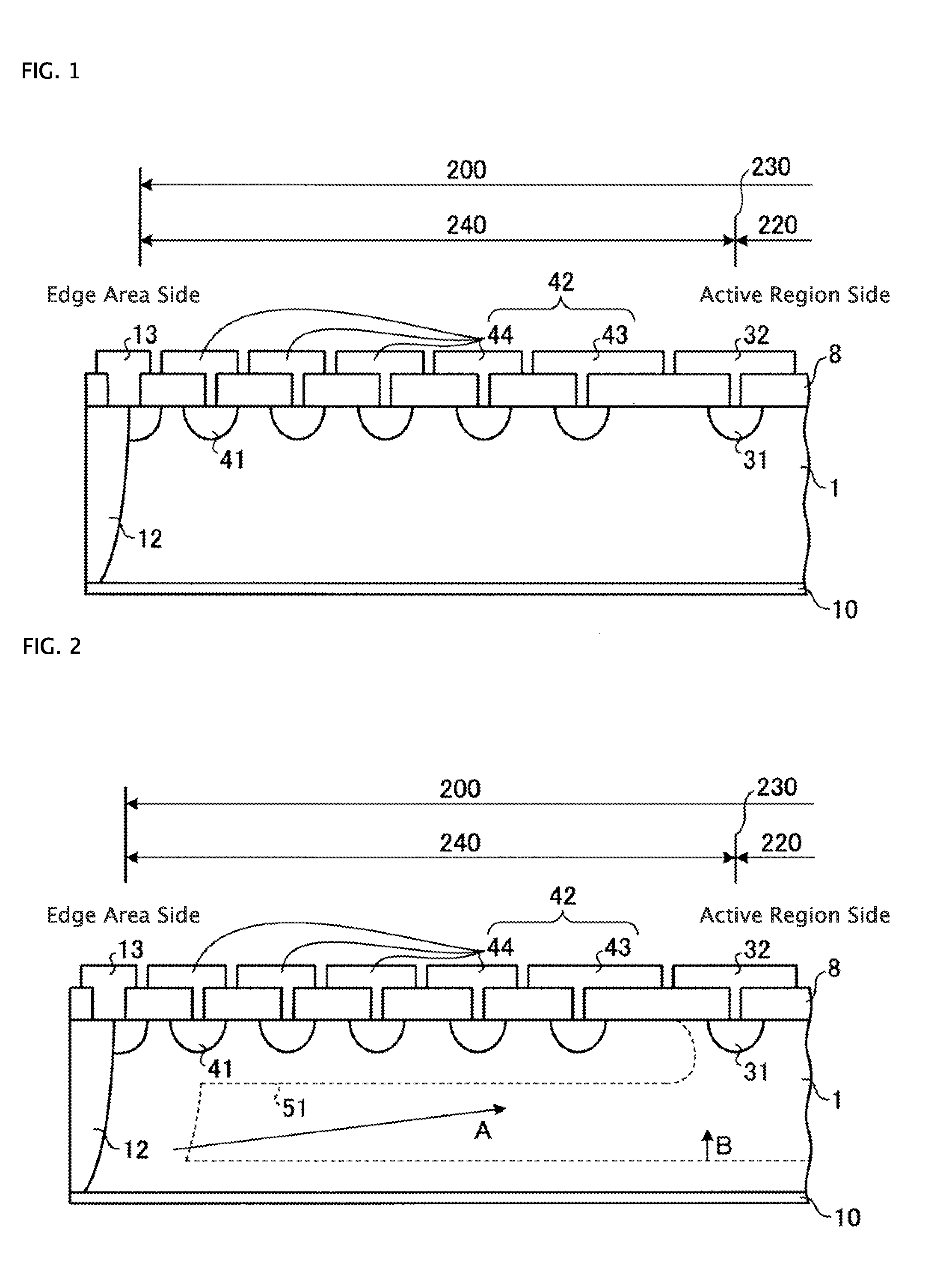
The reverse blocking insulated gate bipolar transistor (hereinafter referred to as the “reverse blocking IGBT”) according to a first embodiment of the invention includes a semiconductor substrate including an n-type (a first conductivity type) drift region; an active region in the semiconductor substrate; a breakdown-withstanding junction edge-termination region (hereinafter referred to simply as a “breakdown withstanding region”) outside the active region; and a p-type (a second conductivity type) separation region in the peripheral area of the breakdown withstanding region. In other words, the reverse blocking IGBT according to the first embodiment has a structure, in which the breakdown withstanding region is formed between an emitter region in the active region and the separation region. The breakdown withstanding region relaxes the electric field strength on a pn-junction constituting the semiconductor device and realizes a desired withstand voltages. The drift region correspon...

second embodiment

In the reverse blocking IGBT according to the first embodiment, a semiconductor substrate irradiated with an electron beam may be used. A thermal treatment may be conducted on the semiconductor substrate after the electron beam irradiation. The other structures are the same with the reverse blocking IGBT structures according to the first embodiment (cf. FIG. 1).

According to the second embodiment, an electron beam may be irradiated at the acceleration voltage of 4.8 MeV and at the dose of 20 kGy or higher to the semiconductor substrate used for manufacturing a reverse blocking IGBT. The electron beam irradiation may be conducted on the entire semiconductor substrate. By irradiating an electron beam to the entire semiconductor substrate, crystal defects (lattice defects) may be introduced intentionally into the semiconductor substrate. The thermal treatment after the electron beam irradiation may be conducted at 300 to 380° C. for around 1 hr. By conducting a thermal treatment after t...

third embodiment

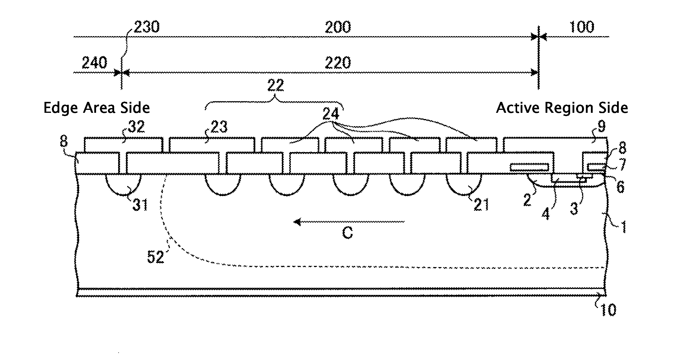
FIG. 6 is a cross sectional view showing the breakdown-withstanding junction edge-termination region in a reverse blocking IGBT according to a third embodiment of the invention.

As shown in FIG. 6, the breakdown withstanding structure in the reverse breakdown withstanding region in the reverse blocking IGBT according to the first embodiment (cf. FIG. 1) may be applied to the forward breakdown withstanding region that obtains mainly a forward withstand voltage when a voltage is applied in the forward direction.

As shown in FIG. 6, forward breakdown withstanding region 220 is formed on the active region 100 side in breakdown-withstanding junction edge-termination region (hereinafter referred to simply as “breakdown withstanding region”) 200. More in detail, in breakdown withstanding region 200, forward breakdown withstanding region 220 is formed between active region 100 and middle section 230 of reverse breakdown withstanding region 240 and forward breakdown withstanding region 220. In...


PUM


Abstract

A reverse blocking IGBT according to the invention can include a reverse breakdown withstanding region, p-type outer field limiting rings formed in a reverse breakdown withstanding region and an outer field plate connected to the outer field limiting rings, the outer field plate including a first outer field plate in contact with outer filed limiting rings nearest to the active region and second outer field plates in contact with other outer field limiting rings. The first outer field plate having an active region side edge portion projecting toward the active region and second outer field plate having an edge area side edge portion projecting toward the edge area. The reverse blocking IGBT according to the invention can facilitate improving the withstand voltages thereof and reducing the area thereof.

Description

BACKGROUND OF THE INVENTIONA. Field of the InventionThe present invention relates to semiconductor devices.B. Description of the Related ArtIn the field of electric power converters using a semiconductor device, matrix converters have been known to the persons skilled in the art as direct converter circuits which conduct an alternating current to alternating current conversion (hereinafter referred to an “AC / AC conversion”), an alternating current to direct current conversion (hereinafter referred to an “AC / DC conversion”) and a direct current to alternating current conversion (hereinafter referred to as a “DC / AC conversion”).The matrix converter includes AC switches. Since an AC voltage is applied to the AC switches, it is required for the AC switches to exhibit withstand voltages in the forward and reverse directions. In other words, the AC switches are required to exhibit a forward withstand voltage and a reverse withstand voltage. From the view points of reducing the size, weigh...

Claims


Application Information

Patent Timeline
IPC IPC(8): H01L29/739
CPCH01L29/0619H01L29/7395H01L29/7393H01L29/404
Inventor YOSHIKAWA, KOHKUBOUCHI, MOTOYOSHI
Owner FUJI ELECTRIC CO LTD
Why Eureka
Try Eureka