This helps you quickly interpret patents by identifying the three key elements:
Problems solved by technology
Method used
Benefits of technology
Benefits of technology
The patent describes a photodetector that uses a layer of photoelectric conversion material to capture light. The layer has two types of charge carriers that drift through the layer and enter a "multiplication region" where they are amplified using a process called avalanche multiplication. This allows the detector to detect low levels of light. The patent also describes a configuration that reduces variations in electric potential, resulting in a more uniform electric field and increased photosensitivity. Overall, the patent describes a technical solution for improving the detection of light using a detector.
Problems solved by technology
For example, the configuration disclosed in U.S. Pat. No. 8,093,624 is unable to be fabricated by a complementary metaloxide semiconductor (CMOS) process.
This leads to a longer time before the discharge, resulting in a decrease in the photodetection efficiency.
However, a thick photoelectric conversion layer causes a higher avalanche breakdownvoltage in the configurations disclosed in WO 2008 / 004547, WO 2014 / 097519, and Japanese Unexamined Patent Application Publication No. 2015-5752.
Method used
Image
Click on the blue label to locate the original text in one second.
Reading with bidirectional positioning of images and text.
Examples
embodiment 1
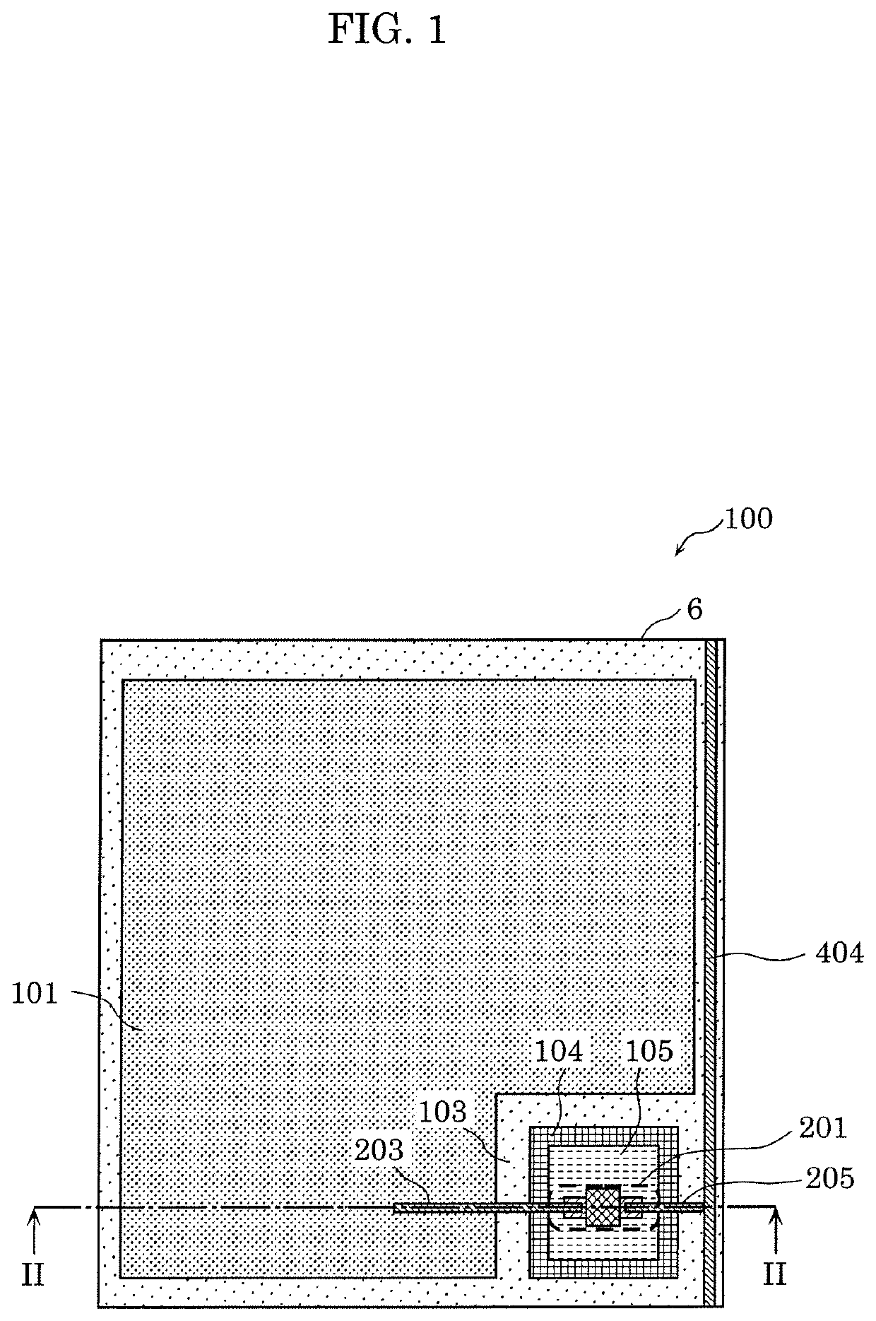
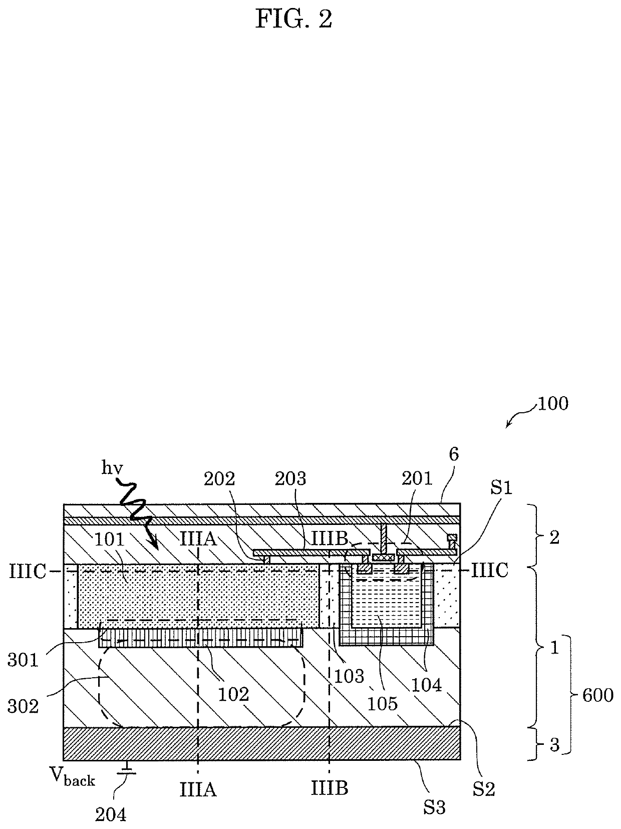
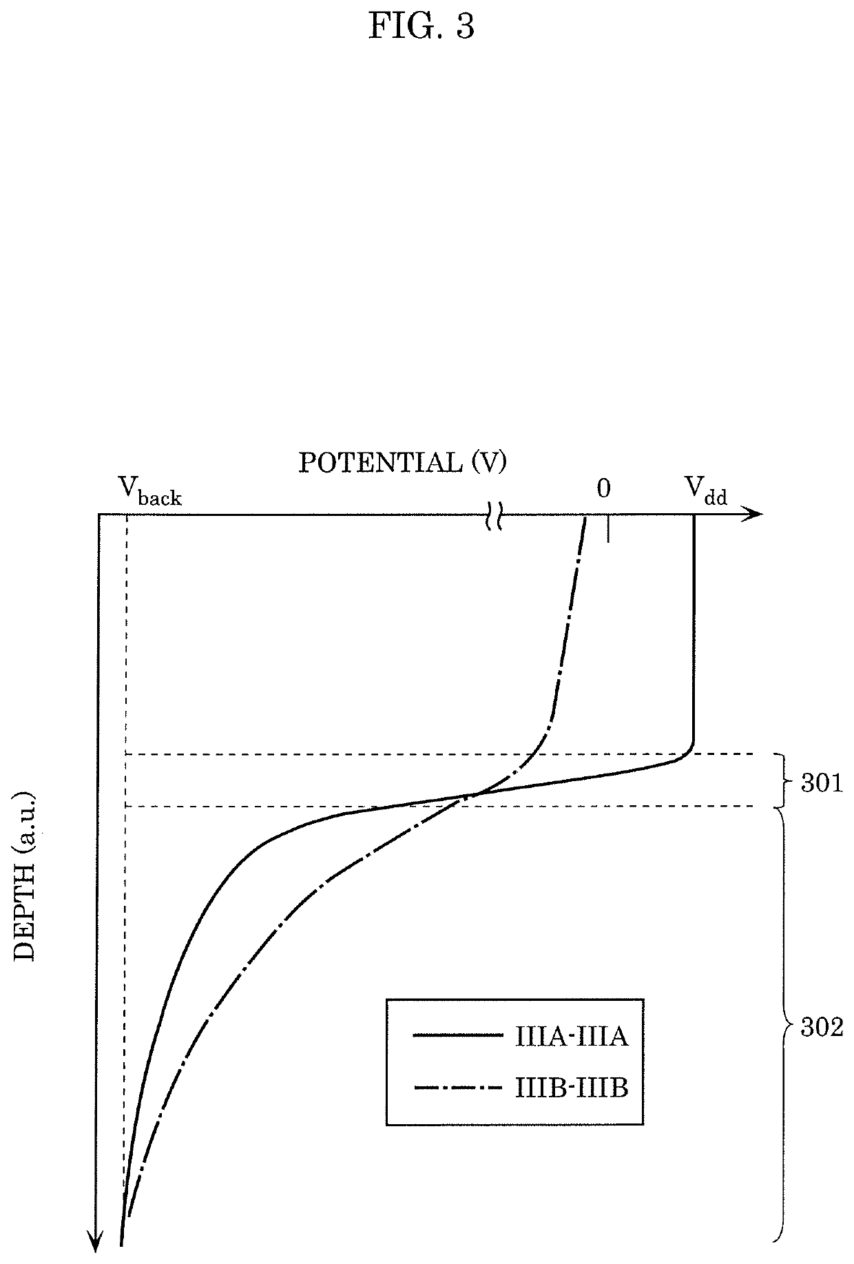
[0160]A configuration of a photodetector according to Embodiment 1 is first described, with reference to FIG. 1 and FIG. 2.
[0161]FIG. 1 is a plan view of photodetector 100 according to Embodiment 1 of the present disclosure. FIG. 2 is a cross-sectional view of photodetector 100 along line II-II of FIG. 1, according to Embodiment 1 of the present disclosure.
[0162]Note that each of FIG. 1 and FIG. 2 illustrates, among structural components included in photodetector 100, pixel 6 that includes first semiconductor layer 101, isolation region 103, first well 104 (circuit region), second well 105 (circuit region), isolation transistor 201, first line 203, and a row signal line that is included in readout circuit 407 (see FIG. 5). Thus, some of the structural components of photodetector 100 are omitted from FIG. 1 and FIG. 2. For example, some of the structural components, such as a line connected to a gate of isolation transistor 201, are omitted from FIG. 1. Note that some of the structur...
embodiment 2
[0224]A configuration of a photodetector according to Embodiment 2 is next described, with reference to FIG. 8 and FIG. 9.
[0225]In the following description on the photodetector according to Embodiment 2, components that are substantially the same as those included in the photodetector according to Embodiment 1 are assigned the same reference marks as used in Embodiment 1, and descriptions on these components may be partially omitted or simplified.
[0226]A peripheral circuit configuration of the photodetector according to Embodiment 2 may be similar to the circuit configuration of photodetector 100 according to Embodiment 1 as illustrated in FIG. 5 for example, and is thus omitted from the description.
[0227]FIG. 8 is a plan view of photodetector 100a according to Embodiment 2 of the present disclosure. FIG. 9 is a cross-sectional view illustrating photodetector 100a along line IX-IX of FIG. 8, according to Embodiment 2 of the present disclosure.
[0228]Second semiconductor layer 102a o...
modification 3
[0282]FIG. 21 is a plan view of the photodetector according to Modification 3 of Embodiment 2 of the present disclosure. FIG. 22 is a cross-sectional view of the photodetector along line XXII-XXII of FIG. 21, according to Modification 3 of Embodiment 2 of the present disclosure.
[0283]Photodetector 1003 includes second conductivity layer 700 in first semiconductor layer 101c of epitaxial layer 1g. Second conductivity layer 700 is different in conductivity type from first semiconductor layer 101c. To be more specific, photodetector 1003 includes second conductivity layer 700, which is of the second conductivity type, in first semiconductor layer 101c that is closer to first main surface S1 than multiplication region 301 in semiconductor substrate 601. Even more specifically, first semiconductor layer 101c includes second conductivity layer 700 that is in contact with first main surface S1 of semiconductor substrate 601.
[0284]Second conductivity layer 700 is connected to contact 701 (e...
PUM
Abstract
A photodetector includes: a semiconductor substrate having a first main surface and a second main surface; a first semiconductor layer that is of a first conductivity type, and is included in the semiconductor substrate and closer to the first main surface than to the second main surface; a second semiconductor layer that is of a second conductivity type different from the first conductivity type, and is included in the semiconductor substrate and interposed between the first semiconductor layer and the second main surface; a multiplication region that causes avalanche multiplication to a charge generated in the semiconductor substrate through photoelectric conversion; a circuit region disposed alongside the first semiconductor layer in a direction parallel to the first main surface; at least one isolation transistor disposed in the circuit region; and an isolation region interposed between the first semiconductor layer and the circuit region.
Description
CROSS REFERENCE TO RELATED APPLICATIONS[0001]This application is a U.S. continuation application of PCT International Patent Application Number PCT / JP2019 / 013885 filed on Mar. 28, 2019, claiming the benefit of priority of Japanese Patent Application Number 2018-067892 filed on Mar. 30, 2018, the entire contents of which are hereby incorporated by reference.BACKGROUND1. Technical Field[0002]The present disclosure relates to photodetectors.2. Description of the Related Art[0003]In recent years, highly sensitive photodetectors have been used in various fields, such as medicine, communications, biology, chemistry, surveillance, in-vehicle technology, and radiation detection. As a means to enhance sensitivity, avalanche photodiodes (hereinafter, also referred to as APDs) are used. With an APD, photodetection sensitivity is enhanced through multiplication performed, using avalanche breakdown, on a signal charge generated by photoelectrically converting light incident on a photoelectric co...
Claims
Application Information
Patent Timeline
Application Date:The date an application was filed.
Publication Date:The date a patent or application was officially published.
First Publication Date:The earliest publication date of a patent with the same application number.
Issue Date:Publication date of the patent grant document.
PCT Entry Date:The Entry date of PCT National Phase.
Estimated Expiry Date:The statutory expiry date of a patent right according to the Patent Law, and it is the longest term of protection that the patent right can achieve without the termination of the patent right due to other reasons(Term extension factor has been taken into account ).
Invalid Date:Actual expiry date is based on effective date or publication date of legal transaction data of invalid patent.

