Anode holder, and plating apparatus

Pending Publication Date: 2022-09-29
EBARA CORP
View PDF0 Cites 0 Cited by
  • Summary
  • Abstract
  • Description
  • Claims
  • Application Information

AI Technical Summary

Benefits of technology

[0009]The present invention has been developed in view of the above problems, and one of objects thereof is to provide an anode holder capable of reducing consumption of an additive in a plating apparatus, and a plating apparatus.
[0010]According to an embodiment of the present invention, an anode holder for holding an anode for use in a plating apparatus is provided, and the anode holder includes an inner space formed in the anode holder, to house the anode, a mask including a plurality of holes, and configured to cover a front surface of the inner space, and a diaphragm, at least part of the diaphragm being fixed to the mask in a region of the mask that covers the front surface of the inner space. According to this anode holder, the mask can reduce a region where the diaphragm is in contact with a plat

Problems solved by technology

There is a problem that, when the additive is decomposed, the additive loses the above-described effects, and a desired film cannot be obtained on the substr

Method used


Image

  • Anode holder, and plating apparatus
  • Anode holder, and plating apparatus
  • Anode holder, and plating apparatus

Examples


Example

First Embodiment

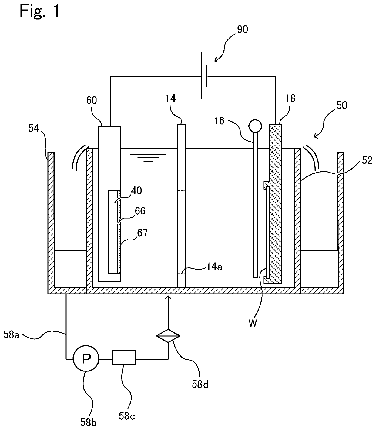
[0037]FIG. 1 is a schematic view showing a plating apparatus according to a first embodiment. As shown in FIG. 1, the plating apparatus includes a plating solution tank 50 holding a plating solution inside, an anode 40 disposed in the plating solution tank 50, an anode holder 60 holding the anode 40, and a substrate holder 18. The substrate holder 18 removably holds a substrate W such as a wafer, and is configured to immerse the substrate W into the plating solution in the plating solution tank 50. The plating apparatus according to the present embodiment is an electroplating apparatus that applies current through the plating solution to plate a surface of the substrate W with a metal.

[0038]The substrate W is, for example, a semiconductor substrate, a glass substrate, or a resin substrate. The metal with which the surface of the substrate W is plated is, for example, copper (Cu), nickel (Ni), tin (Sn), Sn—Ag alloy, or cobalt (Co).

[0039]The anode 40 and the substrate ...

Example

Second Embodiment

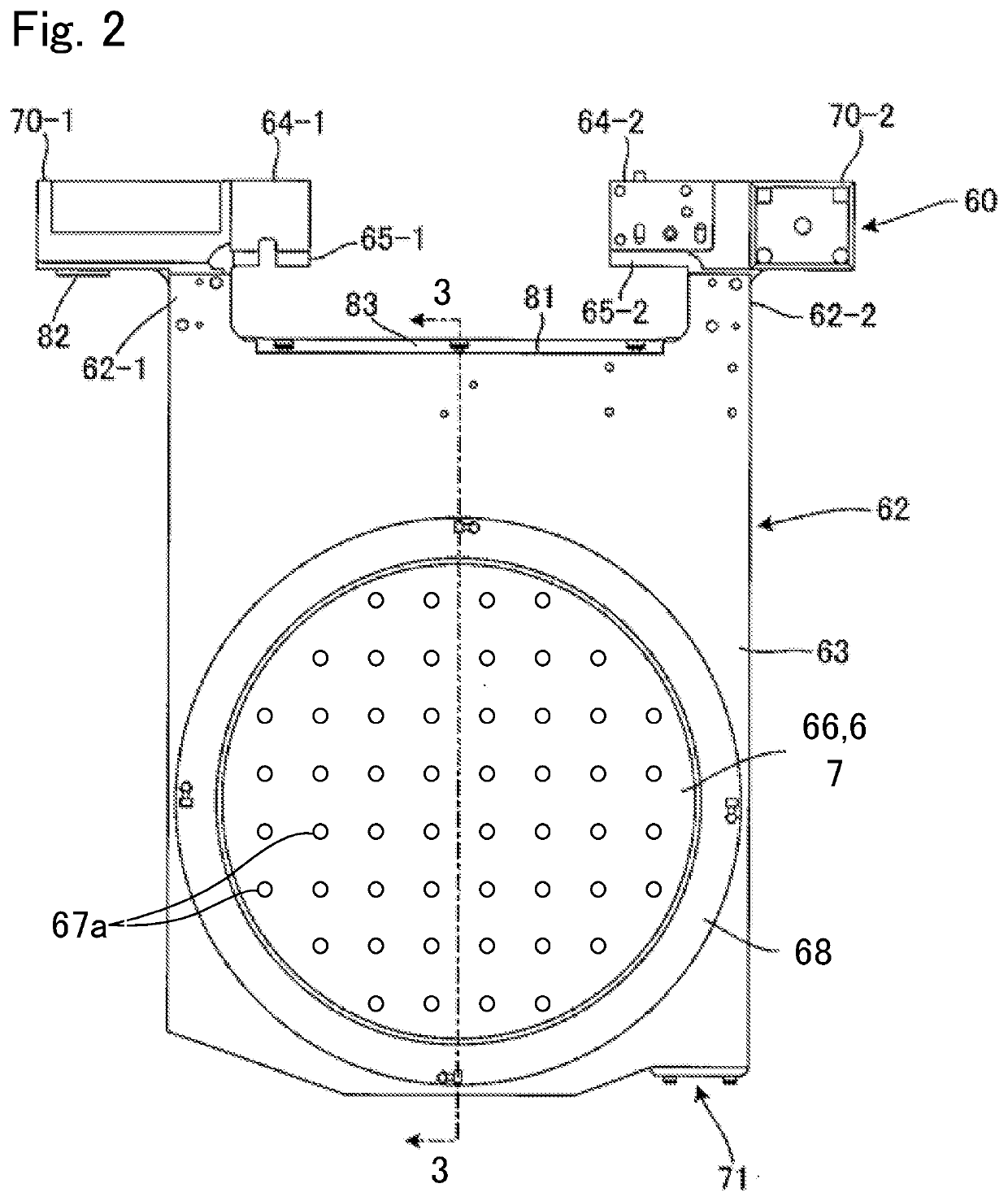
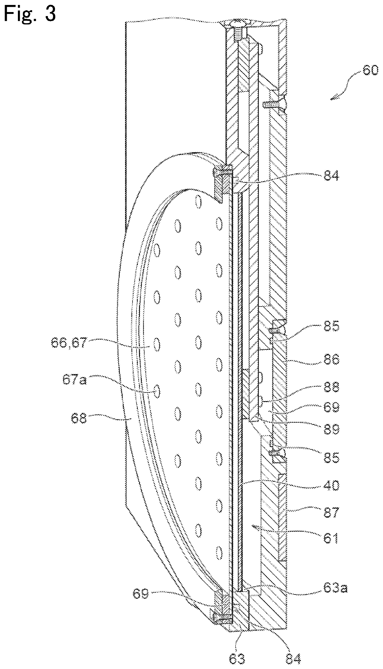
[0084]FIG. 22 is a schematic view showing a plating apparatus according to a second embodiment. The plating apparatus according to the second embodiment is different from the plating apparatus according to the first embodiment in that a diaphragm 66 and a mask 67 are not attached to an anode holder 60, but are mounted in an opening 14a in a regulation plate 14. In the following description, a description that overlaps with that of the first embodiment will not be repeated.

[0085]In the plating apparatus according to the second embodiment, a shield box 160 is disposed in a plating solution storage tank 52, and accordingly, an interior of the plating solution storage tank 52 is divided into an anode tank 170 inside the shield box 160 and a cathode tank 172 outside the shield box. In the example shown in FIG. 22, the anode holder 60 holding an anode 40 and the regulation plate 14 are arranged in the anode tank 170, and a paddle 16 and a substrate holder 18 (cathode) are...

Example

Third Embodiment

[0092]FIG. 23 is a schematic view showing a plating apparatus according to a third embodiment. The plating apparatus according to the third embodiment includes a shield box 160, and a diaphragm 66 and a mask 67 are mounted in an opening 14a in a regulation plate 14, in the same manner as in the second embodiment. The plating apparatus according to the third embodiment is different from the plating apparatus according to the second embodiment in a configuration concerning a plating solution storage tank 52 and the shield box 160, and is the same as the plating apparatus according to the second embodiment in the other respects. In the following description, a description that overlaps with that of the second embodiment will not be repeated.

[0093]In the plating apparatus according to the third embodiment, a bottom plate 51 is disposed in a plating solution storage tank 52, and an interior of the plating solution storage tank 52 is divided, by this bottom plate, into an ...


PUM


Abstract

Provided are an anode holder capable of reducing consumption of an additive in a plating apparatus, and a plating apparatus. An anode holder for holding an anode for use in a plating apparatus is provided, and the anode holder includes an inner space formed in the anode holder, to house the anode, a mask including a plurality of holes, and configured to cover a front surface of the inner space, and a diaphragm, at least part of the diaphragm being fixed to the mask in a region of the mask that covers the front surface of the inner space.

Description

TECHNICAL FIELD[0001]The present invention relates to an anode holder and a plating apparatus.BACKGROUND ART[0002]Heretofore, a wiring has been formed in a fine wiring groove, hole or resist opening provided in a surface of a semiconductor wafer or the like, and a bump (a protruding electrode) to be electrically connected to an electrode of a package or the like has been formed on the surface of the semiconductor wafer or the like. As a method of forming this wiring and bump, for example, an electroplating method, an evaporation method, a printing method, a ball bump method or the like is known, but with increase in an I / O number of semiconductor chips and for a finer pitch, the electroplating method is becoming often used in which miniaturization is possible and performance is relatively stable.[0003]A plating apparatus for use in the electroplating method includes a substrate holder holding a substrate of a semiconductor wafer or the like, an anode holder holding an anode, and a p...

Claims


Application Information

Patent Timeline
IPC IPC(8): C25D17/00C25D17/02C25D17/10
CPCC25D17/002C25D17/02C25D17/10C25D17/001C25D21/04C25D7/12C25D17/12C25D21/12C25D17/004C25D17/008C25D17/06C25D5/022
Inventor KANDA, HIROYUKIIKEDA, HIRONARIKIMURA, MASAAKINAGAI, MIZUKI
Owner EBARA CORP
Why Eureka
Try Eureka