Methods for conducting current between a scanned-probe and storage medium

a technology of conducting current and scanning probe, which is applied in the field of data storage devices, can solve the problems of vacuum requirement, requiring more complicated and expensive manufacturing techniques to focus electron beams, and different magnitude of signal current traveling across the photodiode interfa

Inactive Publication Date: 2007-01-30
HEWLETT PACKARD DEV CO LP
View PDF43 Cites 11 Cited by
  • Summary
  • Abstract
  • Description
  • Claims
  • Application Information

AI Technical Summary

Benefits of technology

[0038]Certain embodiments of the present invention allow for the effect of variations in the distance between the emitters 3

Problems solved by technology

Therefore, it is sometimes necessary to incorporate electron optics, often requiring more complicated and expensive manufacturing techniques to focus the electron beams.
The changes of state can be caused by the bombarding electrons themselves, specifically when collisions between the electrons and the media atoms rearrange the atoms, but can also be caused by the high-power-density-electron beams transferring the energy of the electrons to the storage areas and causing localized heating.
This leads to a different amount of minority carriers generated in the photodiode by the stimulated photons and results in a dif

Method used


Image

  • Methods for conducting current between a scanned-probe and storage medium
  • Methods for conducting current between a scanned-probe and storage medium
  • Methods for conducting current between a scanned-probe and storage medium

Examples


Embodiment Construction

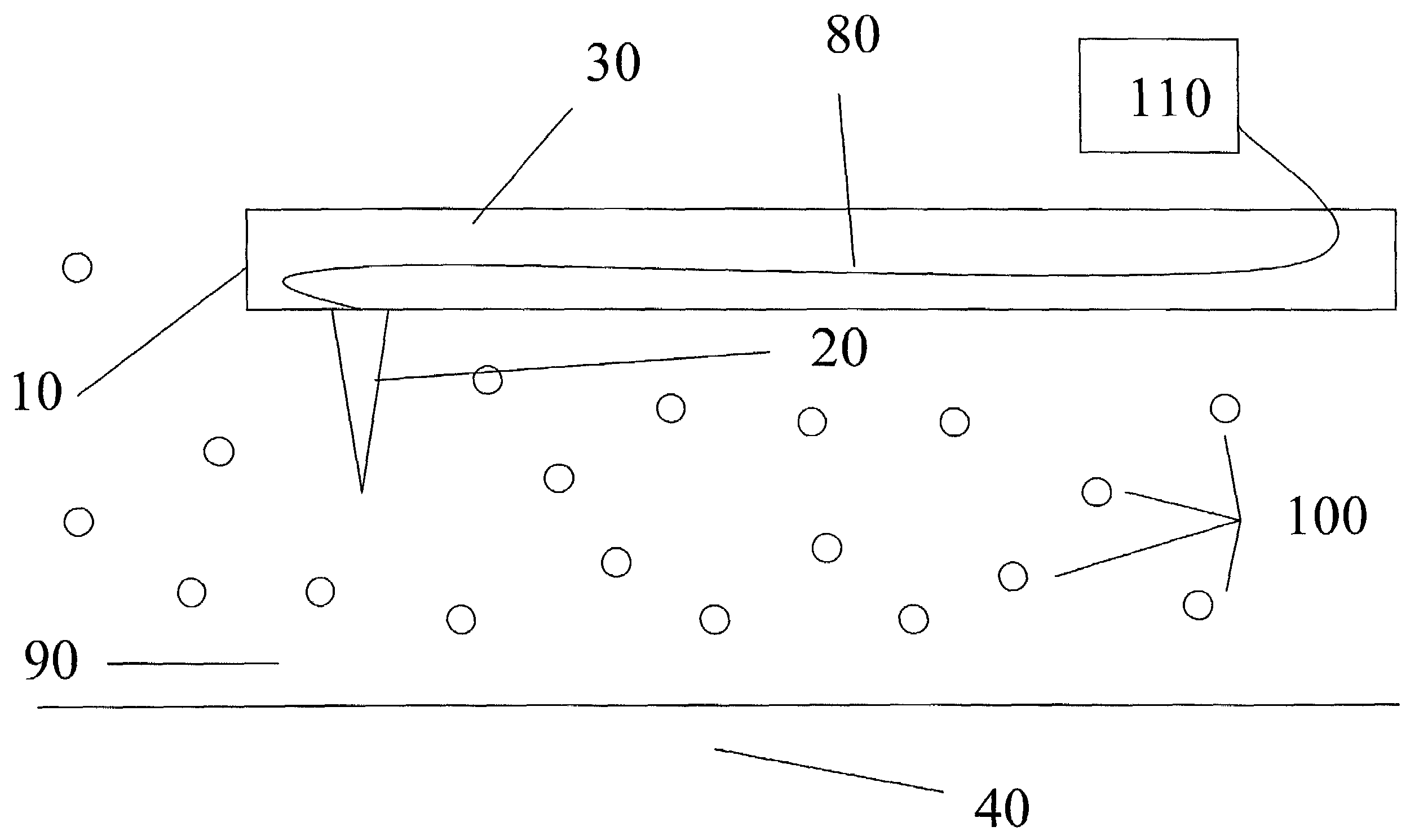
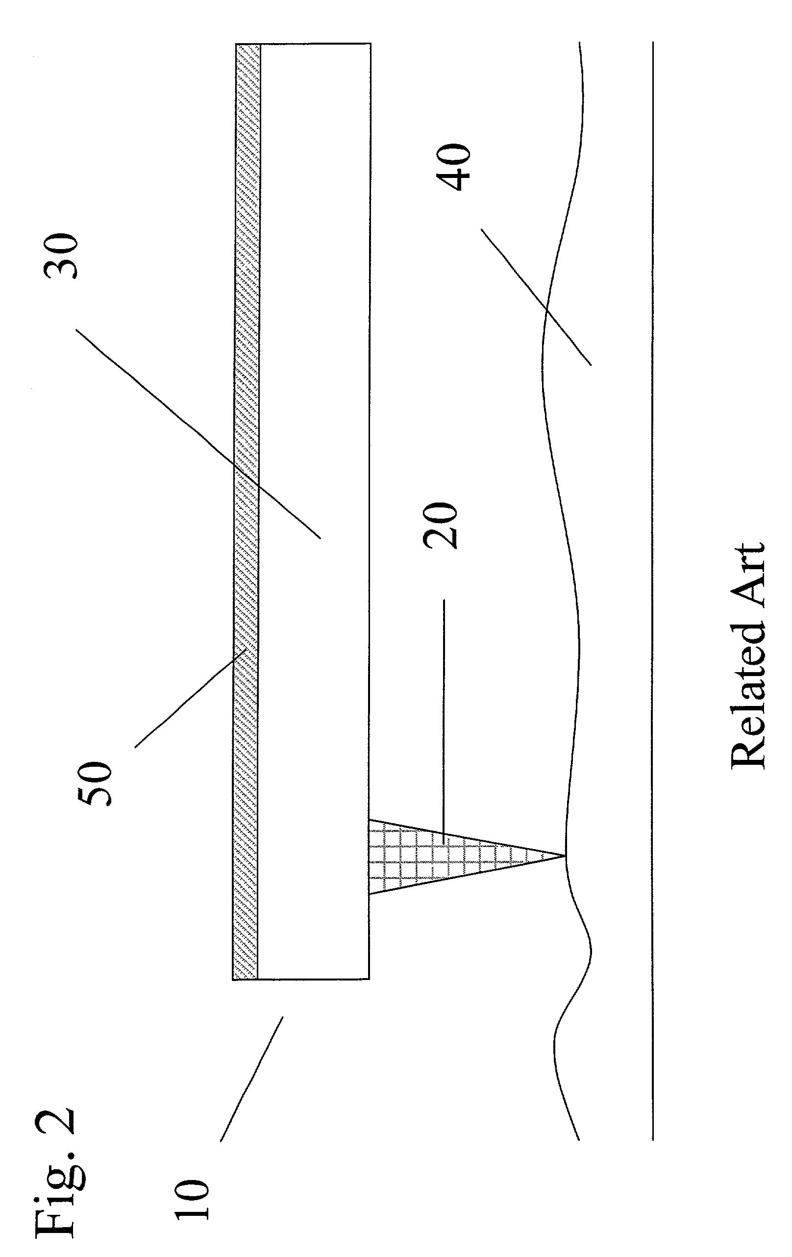
[0048]Certain embodiments of the present invention are illustrated in FIG. 3, wherein a probe 10, made up of a tip 20, a compliant suspension 30, a power source 110 in the “off” position and a connection 80 connecting the tip 20 to the power source 110 are illustrated. A storage medium 40 is illustrated below the probe 10 and a fluid medium 90, with particles 100 floating therein, is illustrated between the storage medium 40 and the probe 10.

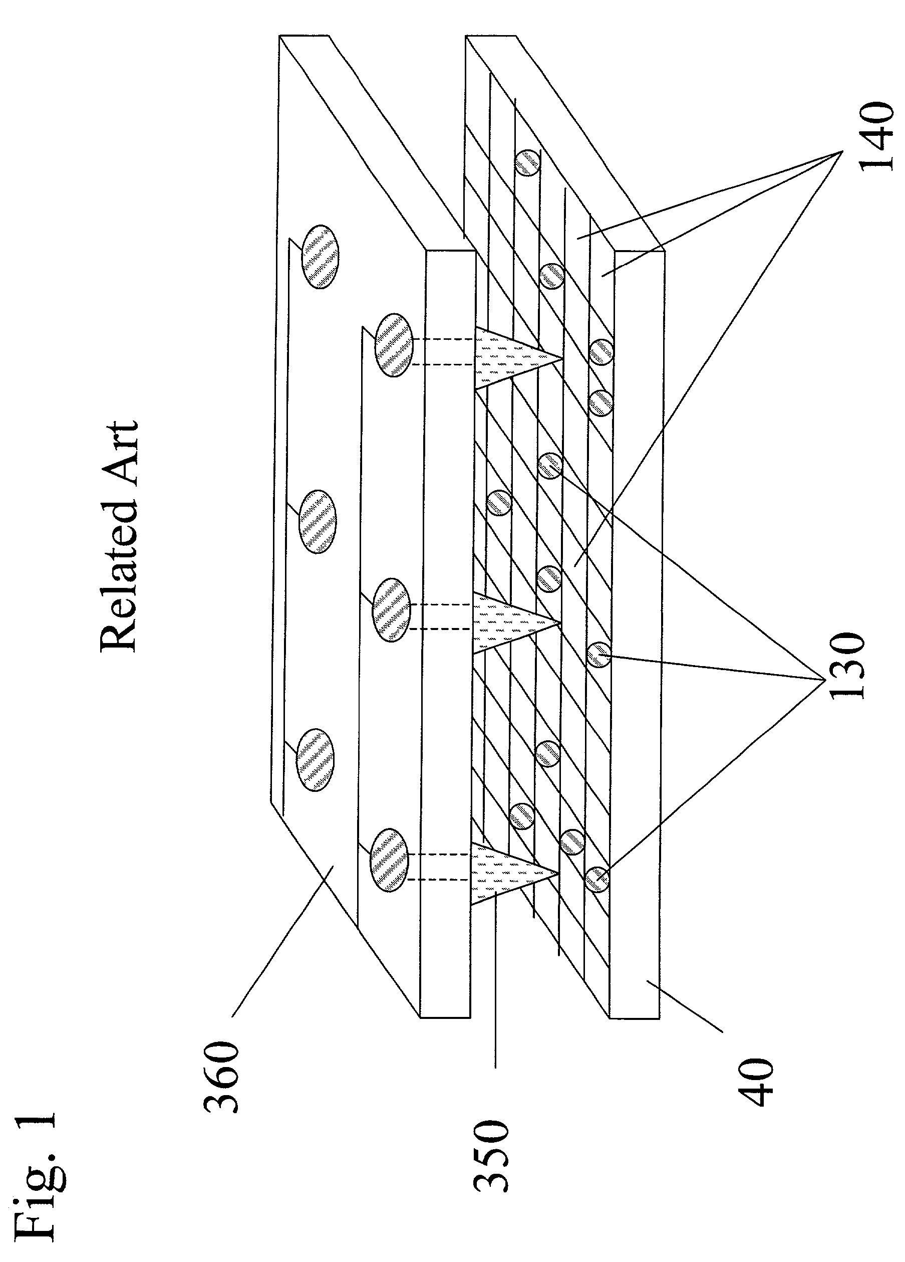
[0049]The probe 10 can be analogous to AFM probes such as, but not limited to, those discussed above. Multiple probes 10 can be attached to an emitter array support 360 such as, but not limited to, those discussed above. The emitter array support 360 to which the probes are attached may be moved relative to the storage medium 40 in order to position the probe 10 over a particular storage area or the storage medium 40 may be moved relative to the emitter array support 360.

[0050]In addition to the emitter array support 360 embodiments discussed in...


PUM


Abstract

Certain embodiments of the present invention are directed at data storage devices capable of storing, reading and writing data to storage areas of nanometer dimensions. Certain embodiments are directed at devices wherein a fluid medium and particles are provided between a storage medium and an energy-emitting tip to channel energy from the tip to the storage medium. Certain embodiments are directed at devices wherein conductor molecules are attached to the surface of the storage medium and channel energy to the storage medium from an energy-emitting tip. Certain embodiments of the present invention are directed at methods of reading and writing to a storage medium by making use of intermediate particles and/or molecules to channel beams from a tip to a storage medium where data is stored.

Description

RELATED APPLICATION[0001]This application is related to U.S. Patent application to Gary Gibson entitled AFM VERSION OF DIODE- AND CATHODOCONDUCTIVITY- AND CATHODOLUMINESCENCE-BASED DATA STORAGE MEDIA, S / N 20020067634, filed Dec. 1, 2000. That application is incorporated herein in its entire by reference.FIELD OF THE INVENTION[0002]The present invention relates to a data storage device capable of storing, reading and writing data to data storage areas of nanometer dimensions.BACKGROUND OF THE INVENTION[0003]Recently, scientists have been developing alternative ultra-high-density data storage devices and techniques useful for operating ultra-high-density data storage devices. These devices and techniques store data bits within storage areas sized on the nanometer scale and possess advantages over conventional data storage devices. Among these advantages are quicker access to the data bits, a lower cost per bit and enablement of the manufacturing of smaller electronic devices.[0004]FIG...

Claims


Application Information

Patent Timeline
IPC IPC(8): G11B9/10B82B3/00G01Q60/32G01Q60/34G01Q80/00G11B5/00G11B7/004G11B9/00G11B33/14
CPCB82Y10/00G11B9/14G11B9/1409G11C13/0014G11B9/1463G11B5/00G11C2213/81G11B33/14G11B2005/0002G11B2005/0005
Inventor GIBSON, GARY A.
Owner HEWLETT PACKARD DEV CO LP
Why Eureka
Try Eureka