
Printed circuit board with low cross-talk noise

a printed circuit board and low cross-talk technology, applied in the direction of conductive pattern formation, association of printed circuit non-printed electric components, electrical apparatus construction details, etc., can solve the problems of reducing noise margins, affecting signal quality, and compromising signal integrity, so as to achieve low cross-talk, high density wiring patterns, and effective operation

Inactive Publication Date: 2007-02-13
WACHOVIA CAPITAL FINANCE NEW ENGLAND AS AGENT +1
View PDF17 Cites 34 Cited by
  • Summary
  • Abstract
  • Description
  • Claims
  • Application Information

AI Technical Summary

Benefits of technology

[0019]It is another object of the invention to provide a PCB which is capable of operating effectively with a minimum of crosstalk while still allowing high density wiring patterns, if desired, e.g., to couple electronic packages such as chip carriers thereto.
[0020]It is another object of the invention to provide a PCB which can be manufactured using present technology and at comparative costs to present methods used to manufacture less complex boards.
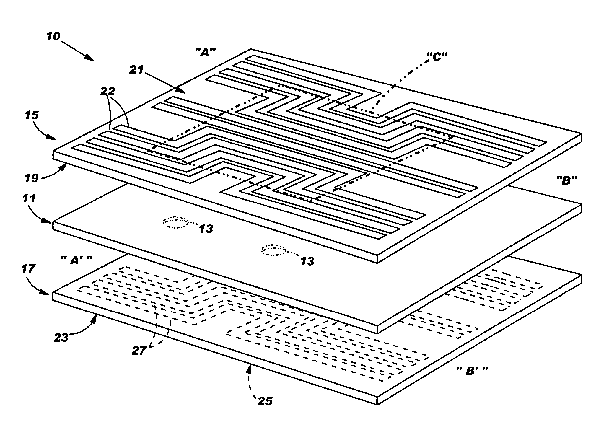
[0021]According to one aspect of the invention, there is provided a printed circuit board comprising a power plane having first and second opposing sides, first and second dielectric layers located on the first and second opposing sides of the power plane, respectively and first and second signal layers located on the first and second dielectric layers, respectively, each of these signal layers including a plurality of substantially parallel signal lines running in a substantially similar direction across the signal layers from a first side of said signal layer to a second side of said signal layer. At least a large portion of the number of signal lines in the first signal layer are aligned with and substantially parallel to a corresponding large portion of signal lines in the second signal layer. The power plane located substantially between these large portions of aligned and substantially parallel signal lines substantially reduces crosstalk between the first and second signal layers.
[0022]According to another aspect of the invention, there is provided a method of making a printed circuit board comprising the steps of providing a power plane having first and second opposing sides, positioning the first and second dielectric layers on the first and second opposing sides of the power plane, respectively, and positioning first and second signal layers on the first and second dielectric layers, respectively. Each of the signal layers includes a plurality of substantially parallel signal lines running in a substantially similar direction across the signal layer from a first side of the signal layer to a second side of the signal layer. At least a large portion of the number of signal lines in the first signal layer are aligned with and substantially parallel to a corresponding large portion of signal lines in the second signal layer, and the power plane is located substantially between these large portions of aligned and substantially parallel signal lines. The result is to substantially reduce crosstalk between the first and second signal layers in the final board product.

Problems solved by technology

If not properly implemented, the reduction in the rise and fall time of high-frequency digital signals propagating within the PCB may lead to a compromise in signal integrity, for example cross-talk noise and signal distortions due to impedance mismatch.
Crosstalk decreases noise margins and degrades signal quality.
This, of course, can be a major limiting factor in communication systems performance.
Therefore, the design of PCBs has become quite a challenging task, especially when designing high-performance and high-density boards.
However, while the capacitor absorbs some of the voltage, a spike still occurs.
However, spacing the analog components from the digital components can waste precious semiconductor space, which is an important consideration in integrated circuit (and PCB) design.

Method used


Image

  • Printed circuit board with low cross-talk noise
  • Printed circuit board with low cross-talk noise
  • Printed circuit board with low cross-talk noise

Examples


Embodiment Construction

[0027]For a better understanding of the present invention, together with other and further objects, advantages and capabilities thereof, reference is made to the following disclosure and appended claims in connection with the above-described drawings. It is understood that like numerals will be used to indicate like elements from FIG. to FIG.

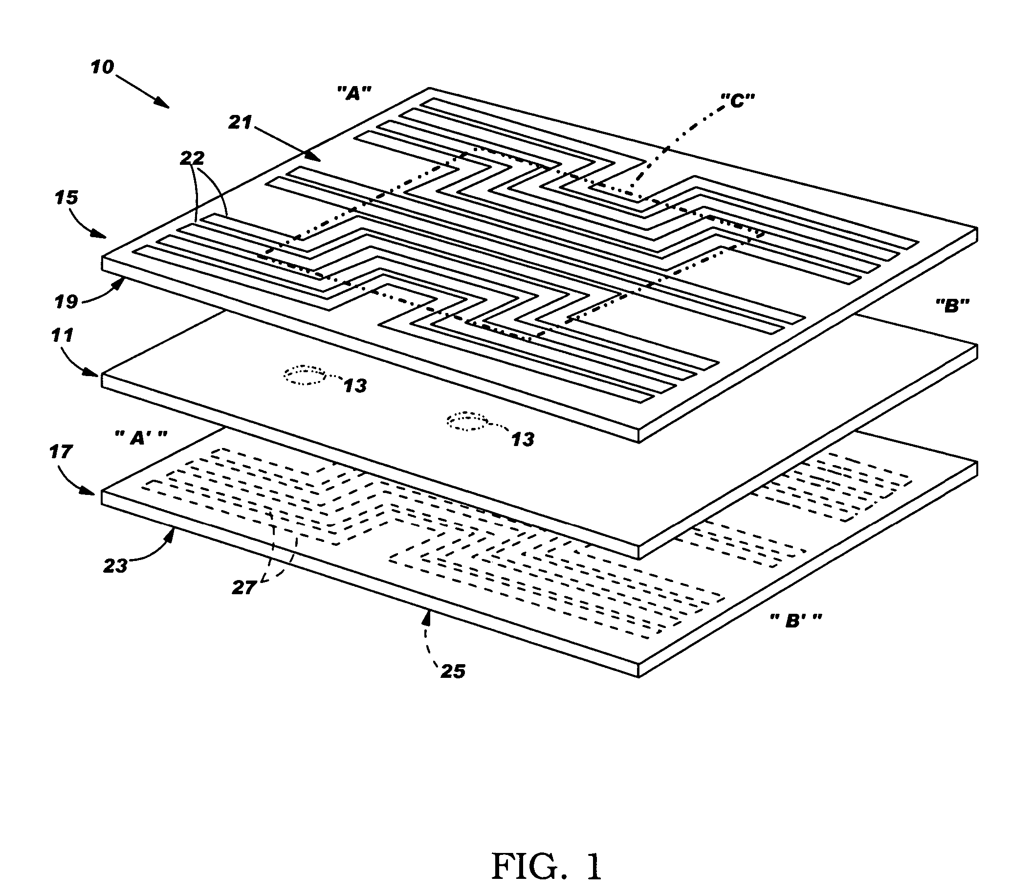
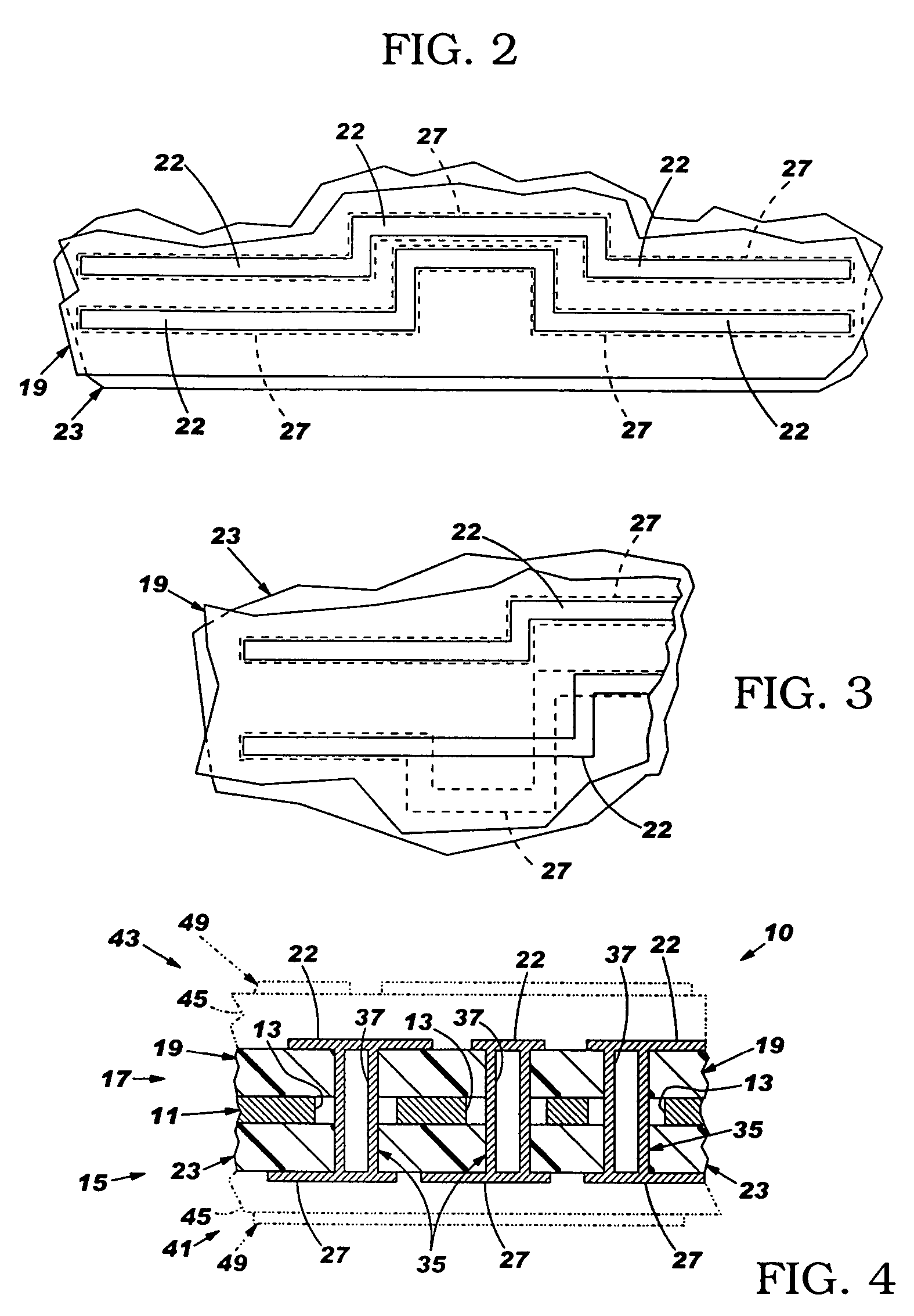
[0028]In FIG. 1, there is shown a printed circuit board (PCB) 10 according to one aspect of the invention. As will be understood from the following description, the resulting structure as defined herein is a PCB with requirements for predominantly singular direction wiring with a reduced number of signal layers having at least equivalent electrical performance to PCBs of the known art, including those of more complex construction. The structure as defined herein allows for internal connections (e.g., internal or “buried” vias to connect adjacent signal layers through the interim power plane) if the structure is to form part of a larger, multilay...


PUM

PropertyMeasurementUnit
thicknessaaaaaaaaaa
pressuresaaaaaaaaaa
temperatureaaaaaaaaaa

Abstract

A printed circuit board and a method of making same in which the board includes a common power plane having dielectric layers on opposing sides thereof and a signal layer on each of said dielectric layers, each signal layer comprising a plurality of substantially parallel signal lines running in substantially similar directions across said signal layers. Predetermined portions of the signal lines in one signal layer are aligned relative to and also parallel to corresponding signal lines in the other signal layer, with the power plane being located between these portions. Through hole connections are provided between selected signal lines in the two layers, these occurring through clearance holes in the power plane so as to be isolated therefrom.

Description

CROSS REFERENCE TO CO-PENDING APPLICATION[0001]This application is a continuation-in-part application of Ser. No. (S.N.) 10 / 354,000, filed Jan. 30, 2003, and now U.S. Pat. 6,828,514.TECHNICAL FIELD[0002]The invention relates to printed circuit (or wiring) boards and particularly to such boards which are adapted for processing high speed signals across various planes thereof.BACKGROUND OF THE INVENTION[0003]Due to technological advances, the need for higher speed circuitries in printed circuit boards (PCBs) have arisen, in turn giving rise to the need for higher speed digital signal transmissions. If not properly implemented, the reduction in the rise and fall time of high-frequency digital signals propagating within the PCB may lead to a compromise in signal integrity, for example cross-talk noise and signal distortions due to impedance mismatch. As the clock frequency of the signal increases, more energy is distributed over the higher frequency spectrum which consequently creates a...

Claims


Application Information

Patent Timeline
Patent Type & Authority Patents(United States)
IPC IPC(8): H05K1/03H05K1/02H05K3/46
CPCH05K1/0216H05K1/0228H05K2201/09236H05K2201/09672Y10T29/4913Y10T29/49117Y10T29/49128Y10T29/49155Y10T29/49126Y10T29/49165
Inventor LAUFFER, JOHN M.MARKOVICH, VOYA R.MCNAMARA, JR., JAMES J.THOMAS, DAVID L.
Owner WACHOVIA CAPITAL FINANCE NEW ENGLAND AS AGENT
Learn More