[0007]It is an object of the invention to provide an improved CMOS operational amplifier of the type including a class AB output stage which provides low noise and fast slewing.
[0008]It is another object of the invention to provide an improved CMOS operational amplifier of the type including a class AB output stage which provides low noise and fast slewing and also provides substantially improved large-signal handling capability, i.e. improved output dynamic range.
[0009]It is another object of the invention to provide a CMOS operational amplifier having reduced quiescent current, low noise, and fast settling time for a large output voltage step.
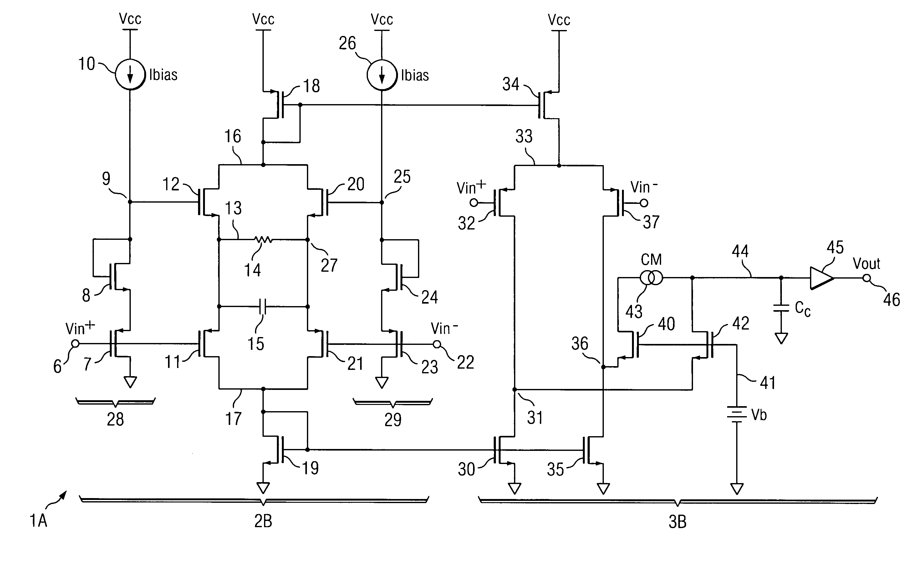
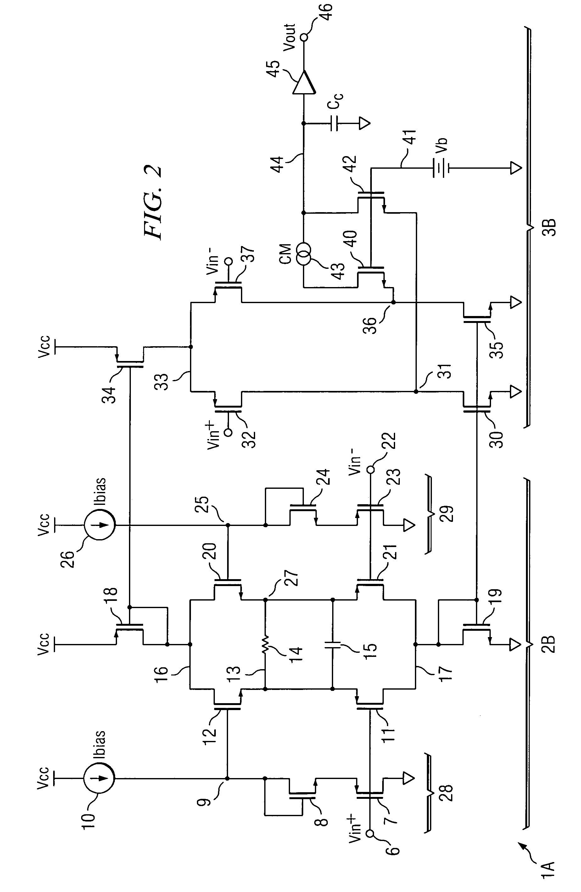
[0012]In one embodiment, the invention provides a method of operating a CMOS amplifier in response to an input signal (Vin) to produce low total harmonic distortion (THD) at high signal frequencies including operating a translinear transconductance stage in response to the input signal (Vin) so as to produce a first current (ID18) having a square-law relationship to the input signal (Vin) and operating a differential input stage of the amplifier including a pair of input transistors (32,37) in response to the input signal (Vin) and operating a tail current source (34) of the differential input stage in response to the first current (ID18) so as to produce a square-law tail current (ID34) proportional to the first current (ID18) in the tail current source (34) to provide input transconductance substantially more constant than is achievable using a constant value of the tail current for the CMOS amplifier for a substantial range of magnitudes of the input signal (Vin).
[0013]In one embodiment, the invention provides a low noise, high slew rate CMOS operational amplifier (1A or 1B) receiving an input signal (Vin) equal to the difference between first (Vin+) and second (Vin−) input signals, the low noise, high slew rate CMOS operational amplifier including a translinear transconductance stage (2B or 2C) including first (12) and second (20) input transistors and third (11) and fourth (21) input transistors, a source of the first input transistor (12) being coupled to a source of the fourth input transistor (21), a source of the second input transistor (20) being coupled to a source of the third input transistor (11), gates of the first (12) and third (11) input transistors being coupled to change in response to the first input signal (Vin+), gates of the second (20) and fourth (21) input transistors being coupled to change in response to the second input signal (Vin−), the translinear transconductance stage being operative to produce a square-law first current (ID18) equal to the sum of drain currents of the first (12) and second (20) input transistors. A folded cascode operational amplifier (3B) includes a differential input stage coupled to receive the input signal (Vin), a folded cascode stage coupled to the differential input stage, and a class AB output stage (45) coupled to the folded cascode stage. The differential input stage receives a tail current equal to or proportional to the square-law first current (ID18) to provide a substantially constant input transconductance of the low noise, high slew rate CMOS operational amplifier for a substantial range of magnitudes of the input signal (Vin).
[0014]In one embodiment, the first (12) and second (20) input transistors have drains coupled to a gate and a drain of a first current source transistor (18), wherein the third (11) and fourth (21) input transistors have drains coupled to a drain of a second current source transistor (19), and wherein the low noise, high-slew-rate CMOS operational amplifier includes a tail current source transistor (34) having a gate coupled to the gate of the first current source transistor (18) so as to cause the tail current source transistor (34) to produce the square-law tail current (ID34) proportional to the first current (ID18).

