Low profile stacking system and method

a stacking system and low profile technology, applied in the direction of printed circuit manufacturing, printed circuit non-printed electric component association, printed circuit aspects, etc., can solve the problems of exposed joint re-melting, solder joint re-melting, unreliability, etc., to achieve low profile, high melting point, and high temperature joints

Inactive Publication Date: 2007-02-20
OVID DATA CO
View PDF311 Cites 60 Cited by
  • Summary
  • Abstract
  • Description
  • Claims
  • Application Information

AI Technical Summary

Problems solved by technology

Typically, however, the formed solder joints will re-melt during subsequent processing.
Common tin-lead solders start to melt at 183° C. and, when exposed to such temperatures and higher, the exposed joint may re-melt and become unreliable.

Method used


Image

  • Low profile stacking system and method
  • Low profile stacking system and method
  • Low profile stacking system and method

Examples


Embodiment Construction

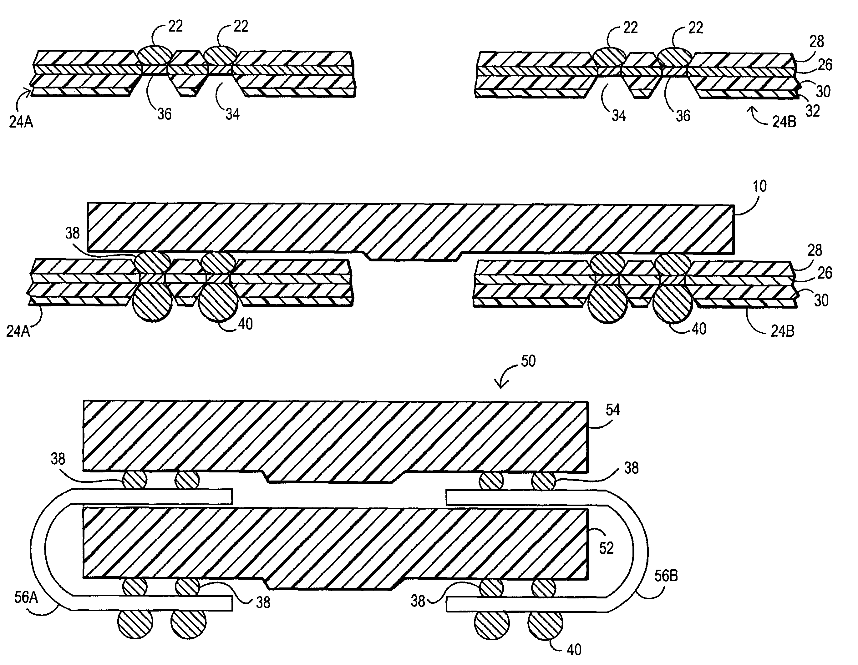
[0014]FIG. 1 depicts an exemplar integrated circuit device 10 having upper surface 11 and lower surface 13. Device 10 is an example of one type of the general class of devices commonly known in the art as chip-scale-packaged integrated circuits (“CSPs”). The present invention may employed with a wide variety of integrated circuit devices and is not, as those of skill in the art will understand, limited to devices having the profile depicted in FIG. 1. Further, although its preferred use is with plastic-bodied CSP devices, the invention provides advantages in mounting a variety of packaged integrated circuit devices in a wide variety of configurations including leaded and CSP topologies.

[0015]Exemplar integrated circuit device 10 may include one or more integrated circuit die and body 12 and a set of contacts 14. The illustrated integrated circuit device 10 has CSP ball contacts 14 arrayed along surface 13 of its body 12. Typically, when integrated circuit device 10 is a CSP device, ...


PUM


Abstract

The present invention provides a system and method that mounts integrated circuit devices onto substrates and a system and method for employing the method in stacked modules. The contact pads of a packaged integrated circuit device are substantially exposed. A solder paste that includes higher temperature solder paste alloy is applied to a substrate or to the integrated circuit device to be mounted. The integrated circuit device is positioned to contact the contacts of the substrate. Heat is applied to create high temperature joints between the contacts of the substrate and the integrated circuit device resulting in a device-substrate assembly with high temperature joints. The formed joints are less subject to re-melting in subsequent processing steps. The method may be employed in devising stacked module constructions such as those disclosed herein as preferred embodiments in accordance with the invention. Typically, the created joints are low in profile.

Description

RELATED APPLICATIONS[0001]The present application is a division of application Ser. No. 10 / 457,608. filed Jun. 9, 2003, which is a continuation-in-part of U.S. patent application Ser. No. 10 / 005,581, filed Oct. 26, 2001, now U.S. Pat. No. 6,576,992, all of which are herein incorporated by reference.TECHNICAL FIELD[0002]The present invention relates to mounting integrated circuit devices on substrates and to mounting integrated circuits on substrates employed in stacked modules.BACKGROUND OF THE INVENTION[0003]A variety of methods are used to mount integrated circuit devices to substrates such as PWBs and flex circuitry. Solder paste is selectively applied to the integrated circuit device or substrate to which the IC is to be attached. The device and substrate are exposed to reflow temperatures of approximately 220° C. The device is, consequently, soldered to the substrate.[0004]Typically, however, the formed solder joints will re-melt during subsequent processing. Common tin-lead so...

Claims


Application Information

Patent Timeline
Patent Type & Authority Patents(United States)
IPC IPC(8): H01L23/02H01L23/31H01L23/498H01L23/538H01L25/065H01L25/10H05K1/14H05K1/18H05K3/36
CPCH01L23/3114H01L23/49816H01L24/13H01L23/49827H01L23/4985H01L23/5387H01L24/10H01L24/81H01L25/0657H01L25/105H05K1/141H05K1/147H01L2924/1305H01L2225/107H01L2224/13099H01L2224/13111H01L2224/16237H01L2224/81191H01L2224/81192H01L2224/81193H01L2224/8121H01L2224/81815H01L2225/06517H01L2225/06541H01L2225/06579H01L2225/06586H01L2924/01029H01L2924/01049H01L2924/01051H01L2924/01075H01L2924/01078H01L2924/01082H01L2924/14H01L2924/15311H01L2924/19041H01L2924/3011H05K1/189H05K3/3463H05K3/363H05K2201/056H05K2201/10689H05K2201/10734H01L2924/01005H01L2924/01006H01L2924/01033H01L2924/01047H01L2924/0105H01L2924/014H01L2924/00H01L24/16H01L2224/13H01L2224/13116H01L2224/73253H01L2224/81011
Inventor PARTRIDGE, JULIANCADY, JAMES W.WILDER, JAMESROPER, DAVID L.WEHRLY, JR., JAMES DOUGLAS
Owner OVID DATA CO
Why Eureka
Try Eureka