Comparing on die response and expected response applied to outputs

a technology of expected response and die response, applied in the field of integrated circuit system and method testing, can solve the problems of limited number of dedicated dies, increased complexity of ics testing, and increased cost for ic manufacturers,

Inactive Publication Date: 2007-02-27
TEXAS INSTR INC
View PDF11 Cites 17 Cited by
  • Summary
  • Abstract
  • Description
  • Claims
  • Application Information

AI Technical Summary

Problems solved by technology

However, as IC circuit density increases, the testing of ICs becomes more complex and costly for the IC manufacturers.
The limitation of the multiple die test arrangement in FIG. 3 lies in the number of dedicated response inputs 305-308 the tester 105 can accept on its response bus.
For example, if the tester can accept 300 response input signals and each die has 100 output pads, the multiple die test arrangement of FIG. 3 is limited to only being able to test 3 die at a time.
The time required to relocate the probe mechanism and repeat the die test say 100 times consumes test time which increases the cost to manufacture the die.
It is possible to widen the response bus input of the tester to say 600 inputs to allow testing 6 die at a time, but adding circuitry to the tester to increase its response bus input width is expensive and that expense would increase the cost of manufacturing die.

Method used


Image

  • Comparing on die response and expected response applied to outputs
  • Comparing on die response and expected response applied to outputs
  • Comparing on die response and expected response applied to outputs

Examples


Embodiment Construction

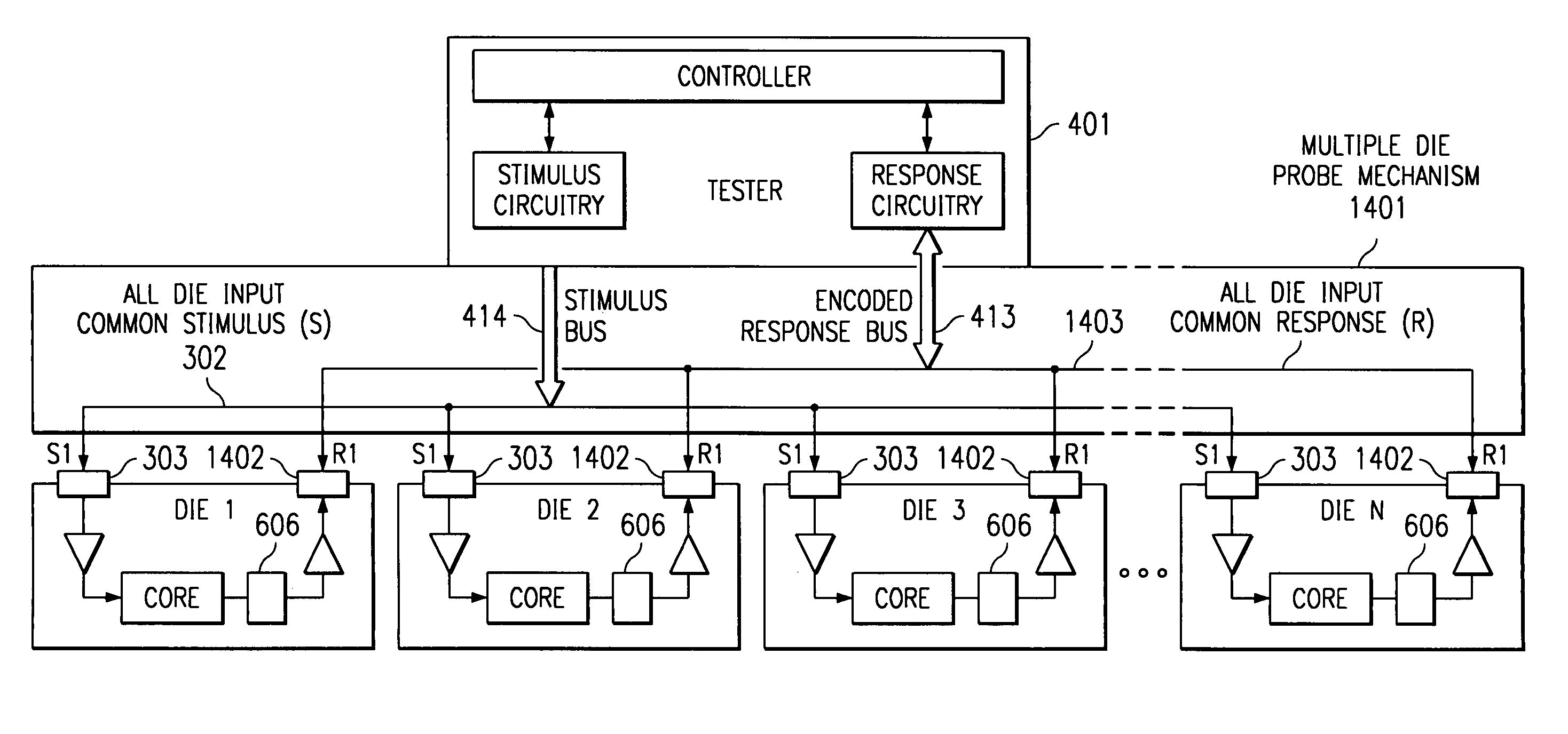
[0046]The present invention, as described in detail below, provides improvements that overcome the limitations stated above using conventional multiple die testing arrangements. Most notably, the present invention provides for significantly increasing the number of die that may be tested in parallel, without having to increase the width of the tester's response bus.

[0047]The present invention improves multiple die testing by; (1) adapting testers to communicate with multiple die using a novel response signaling technique, and (2) adapting the die to be receptive to the tester's novel response signaling technique. Also, the present invention improves connectivity to multiple die on wafer by processing stimulus and response interconnects on the wafer to improve access to multiple die during test. In addition to its ability to improve the testing of multiple die on wafer, the present invention may also be used advantageously to improve the testing of multiple packaged ICs.

[0048]FIG. 4 ...


PUM


Abstract

A test controller applies test stimulus signals to the input pads of plural die on a wafer in parallel. The test controller also applies encoded test response signals to the output pads of the plural die in parallel. The encoded test response signals are decoded on the die and compared to core test response signals produced from applying the test stimulus signals to core circuits on the die. The comparison produces pass / fail signals that are loaded in to scan cells of an IEEE 1149.1 scan path. The pass / fail signals then may be scanned out of the die to determine the results of the test.

Description

CROSS REFERENCE TO RELATED APPLICATIONS[0001]This application is a divisional of application Ser. No. 09 / 896,467, filed Jun. 29, 2001, now U.S. Pat. No. 6,717,429, issued Apr. 6, 2004, which claimed priority under 35 USC 119(e) (1) of provisional application Ser. No. 60 / 215,247, filed Jun. 30, 2000.FIELD OF THE INVENTION[0002]The present invention relates generally to integrated circuits and, more particularly, to systems and methods for testing integrated circuits.BACKGROUND OF THE INVENTION[0003]As transistor geometry continues to shrink, more and more functional circuitry may be embedded within integrated circuits (ICs). This trend is beneficial for the electronics industry since it enables development of smaller, lower power electronic consumer products, such as cell phones and hand held computers. However, as IC circuit density increases, the testing of ICs becomes more complex and costly for the IC manufacturers. Reducing the cost of manufacturing ICs is a primary goal for eve...

Claims


Application Information

Patent Timeline
Patent Type & Authority Patents(United States)
IPC IPC(8): G01R31/26G01R31/317G01R31/3185G01R31/319G01R31/3193
CPCG01R31/31703G01R31/31855G01R31/318533G01R31/318566G01R31/31926G01R31/31932G01R31/3177G01R31/318555G06F11/26G01R31/318572G06F11/277G01R31/318544G01R31/318536G01R31/318541G01R31/318511
Inventor WHETSEL, LEE D.
Owner TEXAS INSTR INC
Why Eureka
Try Eureka