Circuit layout methodology using a shape processing application

a shape processing and circuit layout technology, applied in the field of circuit layout methodology, can solve problems such as the increase of chip size, achieve the effects of reducing data volume and masking designs, simplifying design/layout rules, and less complex op

Inactive Publication Date: 2007-03-06
INT BUSINESS MASCH CORP
View PDF10 Cites 193 Cited by
  • Summary
  • Abstract
  • Description
  • Claims
  • Application Information

AI Technical Summary

Benefits of technology

[0015]The present invention provides a technique for eliminating the extra processing time and file-space requirements associated with the OPC of a VLSI design, and can use a layout grid size that is equal to or not much smaller than the dimensions of minimum size feature. A methodology is described that starts with the design rules for a given manufacturing technology and establishes a new set of layer-specific layout grid values. A circuit layout obeying these new grid requirements leads to a significant reduction in data preparation time, cost, and file size. Furthermore, a layout-migration tool can be used to modify an existing layout in order to enforce the new layout grid requirements. The penalty associated with these new grid requirements is that the chip size may increase because of the increased wire width and spacing.
[0023]The present invention greatly simplifies design / layout rules, and has the potential to significantly decrease data volume and mask designs with less complex OPC.

Problems solved by technology

The penalty associated with these new grid requirements is that the chip size may increase because of the increased wire width and spacing.

Method used


Image

  • Circuit layout methodology using a shape processing application
  • Circuit layout methodology using a shape processing application
  • Circuit layout methodology using a shape processing application

Examples


first embodiment

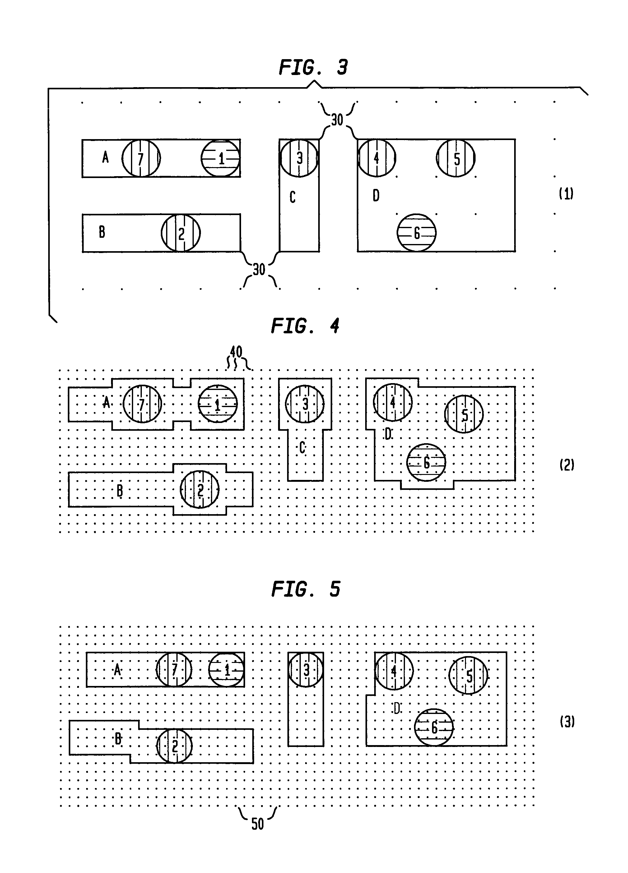
[0089]FIG. 3 shows an illustrative starting first embodiment of the present invention for a 65 nm generation mask having different wire features A, B, C and D, with connecting vias 1, 2, 3, 4, 5, 6 and 7. Note the very large grid size of 100 nm represented by the spaced array of grid points 30. The vias 1–7 are 100 nm diameter and have 0 nm borders, and the wire to wire minimum space is 100 nm.

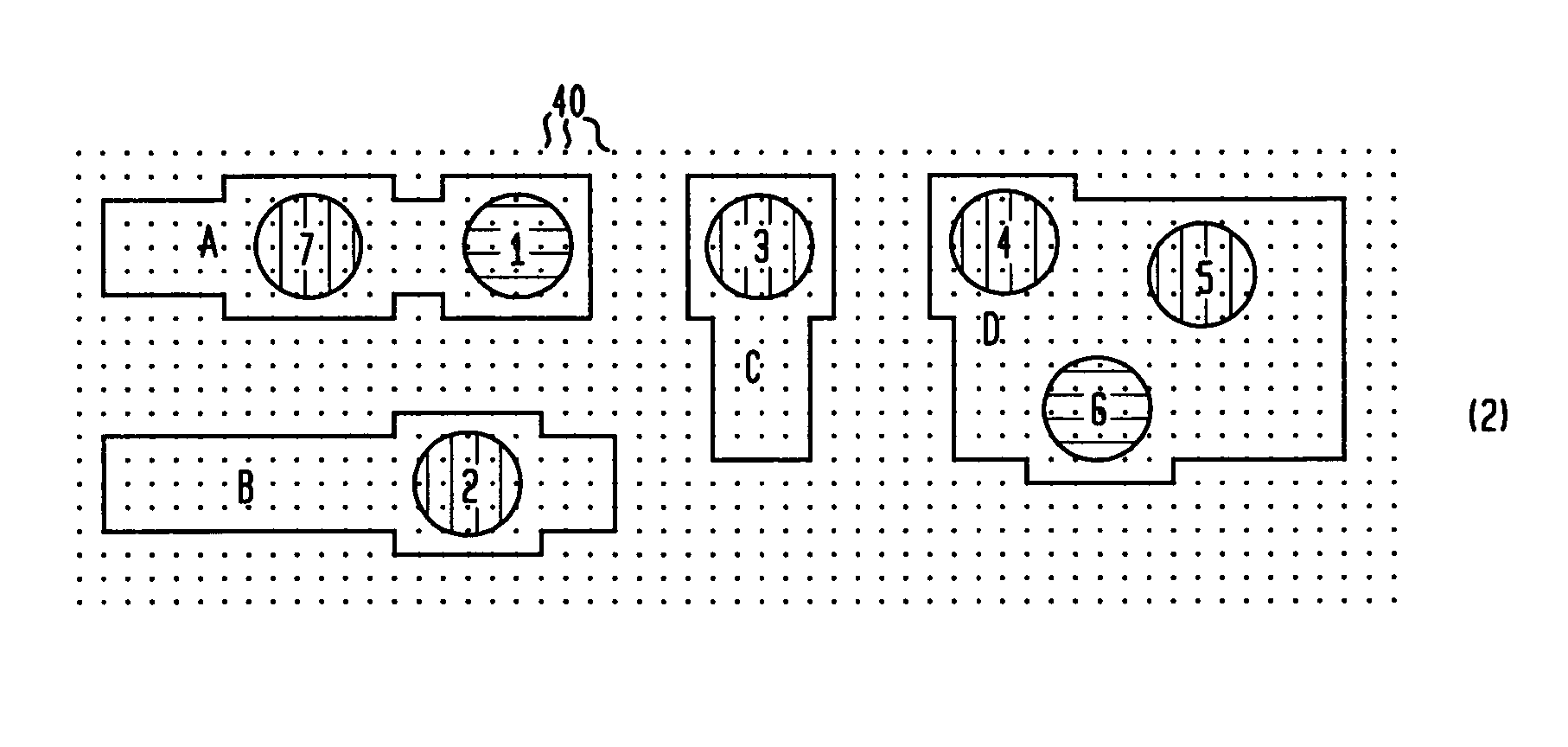
[0090]FIG. 4 illustrates a modified second embodiment (modified relative to embodiment 1) having the same general wire features A–D and same general connecting vias 1–7. Note the relatively smaller grid size of 25 nm represented by the spaced array of grid points 40. The vias 1–7 are 100 nm diameter and have 25 nm borders, and the wire to wire minimum space is 100 nm.

third embodiment

[0091]FIG. 5 illustrates a modified third embodiment having the same general wire features A–D and same general connecting vias 1–7. Note the small grid size of 25 nm represented by the spaced array of grid points 50. The vias 1–7 are 100 nm diameter and have 0 nm borders, and the wire to wire minimum space is 100 nm.

fourth embodiment

[0092]FIG. 6 illustrates a modified fourth embodiment having the same general wire features A–D and same general connecting vias 1–7. Note the small grid size of 25 nm represented by the spaced array of grid points 60. The vias 1–7 are 100 nm diameter and have 25 nm borders, and the wire to wire minimum space is 50 nm.


PUM


Abstract

A circuit layout methology is provided for eliminating the extra processing time and file-space requirements associated with the optical proximity correction (OPC) of a VLSI design. The methodology starts with the design rules for a given manufacturing technology and establishes a new set of layer-specific grid values. A layout obeying these new grid requirements leads to a significant reduction in data preparation time, cost, and file size. A layout-migration tool can be used to modify an existing layout in order to enforce the new grid requirements.

Description

BACKGROUND OF THE INVENTION[0001]1. Field of the Invention[0002]The present invention relates generally to a circuit layout methodology for an integrated circuit (IC), and more particularly pertains to a circuit layout methodology for developing a layout for a very large scale integrated circuit (VLSI) with a set of reduced layout grid ground rules. The circuit layout methodology starts with the design rules for a given technology for fabricating an IC, and establishes a new set of layer-specific layout grid values. A circuit layout obeying these new layout grid requirements leads to a significant reduction in data preparation time, cost, and file size. The present invention can be used for migrating an existing VLSI layout to a set of reduced layout grid ground rules. A layout-migration tool can be used to modify an existing IC layout in order to enforce the new layout grid requirements. A layout-optimization application can be used to rescale data, thus changing the layout grid si...

Claims


Application Information

Patent Timeline
Patent Type & Authority Patents(United States)
IPC IPC(8): G06F17/50
CPCG06F17/5068G06F30/39
Inventor COHN, JOHN M.HIBBELER, JASONSTAMPER, ANTHONY K.RANKIN, JED H.
Owner INT BUSINESS MASCH CORP
Why Eureka
Try Eureka