Method of making a microelectronic package

a microelectronic and package technology, applied in the direction of etching metal masks, printed element electric connection formation, semiconductor/solid-state device details, etc., can solve the problems of time-consuming and expensive electroplating of conductive materials in vias, and achieve the effect of fewer steps and greater flexibility

Inactive Publication Date: 2007-03-13
TESSERA INC
View PDF9 Cites 8 Cited by
  • Summary
  • Abstract
  • Description
  • Claims
  • Application Information

AI Technical Summary

Benefits of technology

[0028]Methods in accordance with embodiments of the invention provide a two-metal component, or a package utilizing a two-metal component, with fewer steps and greater flexibility.

Problems solved by technology

Lining the vias by seeding the vias and then electroplating conductive material in the vias is time consuming and expensive.

Method used


Image

  • Method of making a microelectronic package
  • Method of making a microelectronic package
  • Method of making a microelectronic package

Examples


Embodiment Construction

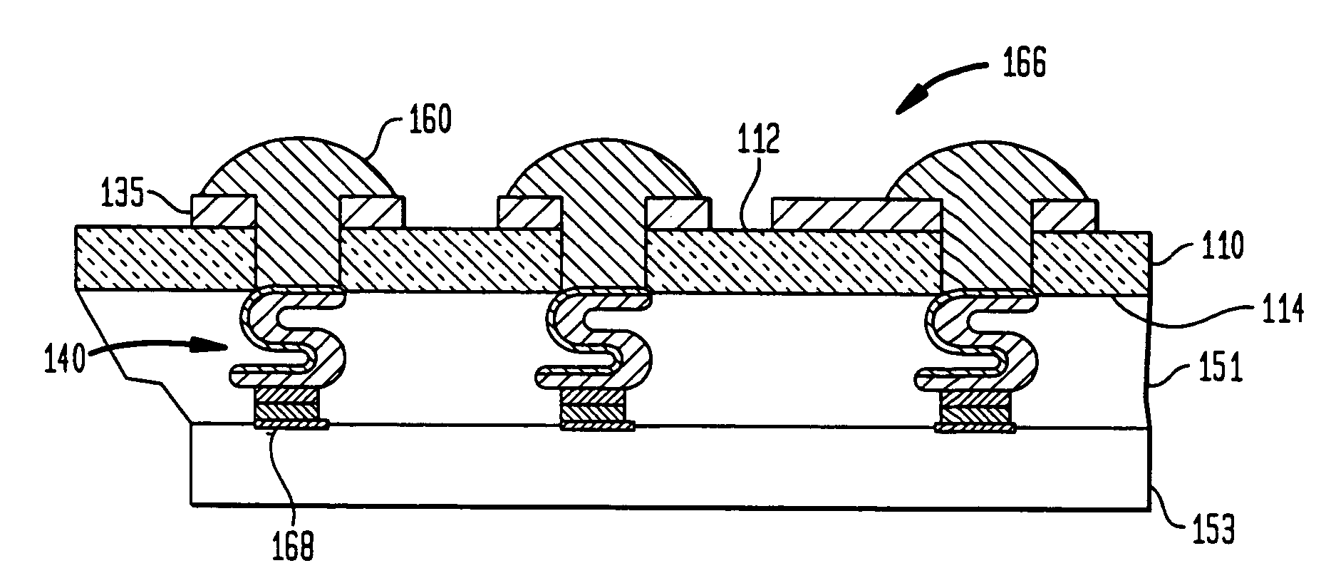
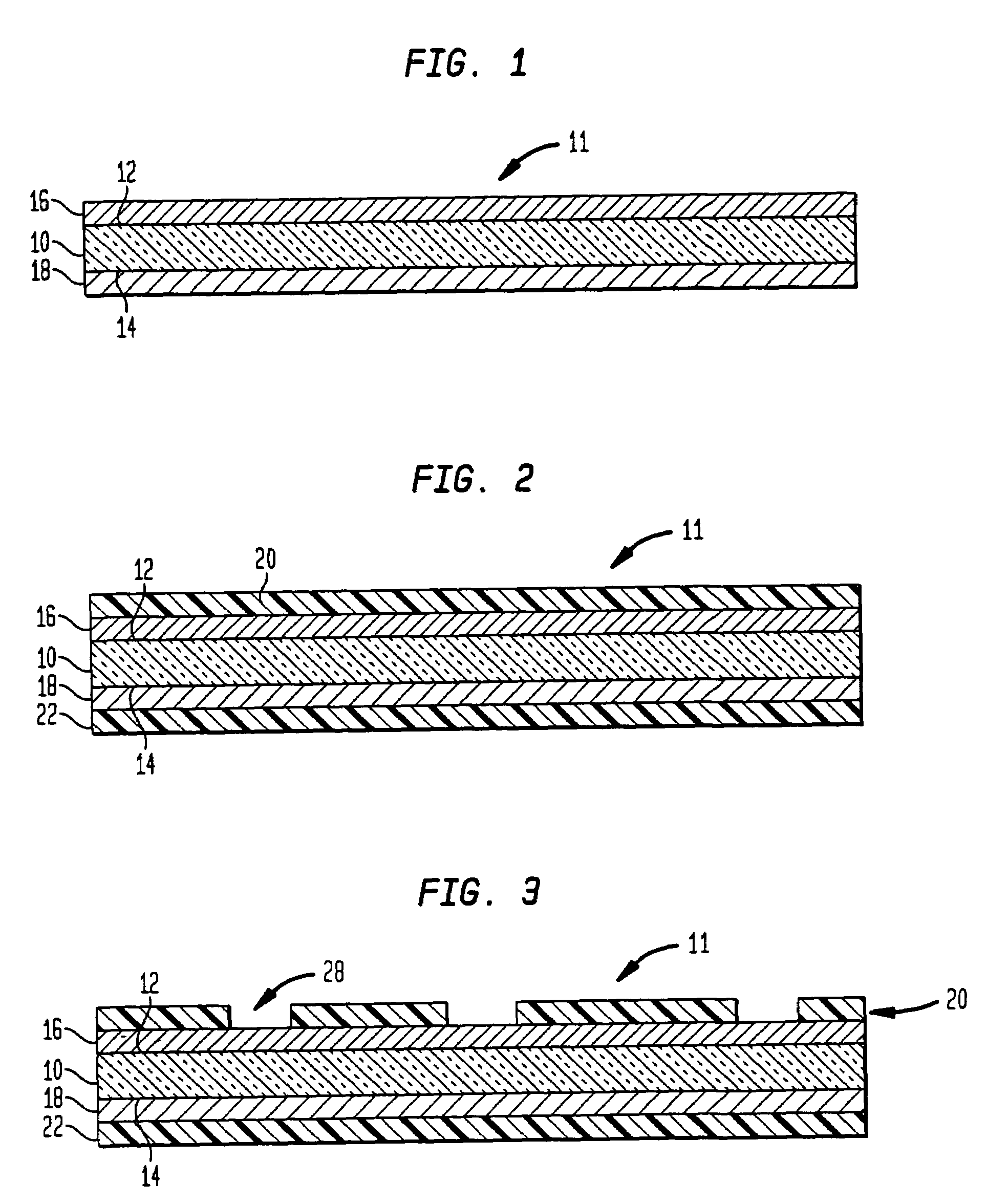
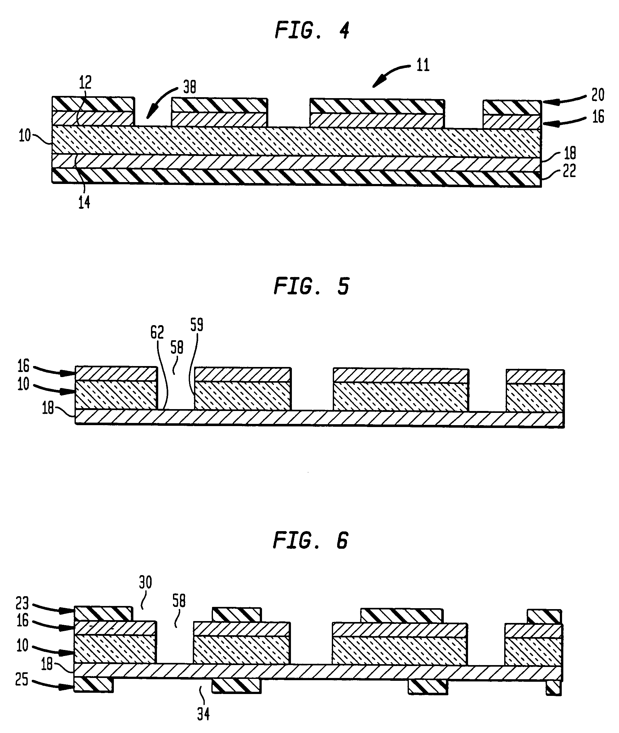
[0065]A method in accordance with an embodiment of the invention is shown in FIGS. 1–17. FIG. 1 shows a structure 11 having a dielectric layer 10 with a top side 12 and a bottom side 14, a top metal layer 16 on the top side 12, and a bottom metal layer 18 on the bottom side 14. As used herein, the terms “top,”“bottom” and other directional terms are to be taken as relative to the microelectronic element, rather than directions based on gravity.

[0066]In certain preferred embodiments, the dielectric layer comprises a sheet of polyimide and the top metal layer and bottom metal layer comprise layers of copper. The top metal layer and bottom metal layer may comprise relatively thin layers of copper, as compared to the thickness of the dielectric layer. For example, the dielectric layer may comprise a layer of polyimide having a thickness of 50 microns and the top metal layer and bottom metal layer may comprise copper layers each having a thickness of 3 microns. Layers of other metals and...


PUM

PropertyMeasurementUnit
thicknessaaaaaaaaaa
thicknessaaaaaaaaaa
thicknessaaaaaaaaaa

Abstract

A microelectronic element is formed from a structure including metal layers on top and bottom sides of a dielectric. Apertures are formed in the top metal layer, and vias are formed in the dielectric in alignment with the apertures. Top and bottom conductive features are formed in proximity to the vias, as by selectively depositing a metal on the metal layers or selectively etching the metal layers. The top and bottom conductive features are connected to one another by depositing a conductive material into the vias, most preferably without seeding the vias as, for example, by depositing solder in the vias.

Description

CROSS-REFERENCE TO RELATED APPLICATIONS[0001]This application is a divisional of U.S. application Ser. No. 09 / 916,554 filed Jul. 27, 2001, now U.S. Pat. No. 6,678,952, which application claims the benefits of Provisional Application No. 60 / 222,868, filed Aug. 3, 2000, the disclosure of which is hereby incorporated by reference herein.FIELD OF THE INVENTION[0002]The present invention relates to methods of making microelectronic packages, and to methods of making microelectronic components for use in fabrication of microelectronic packages.BACKGROUND OF THE INVENTION[0003]Microelectronic elements, such as semiconductor chips, are typically incorporated in a microelectronic package having terminals for forming electrical connections between the semiconductor chip and a second microelectronic element. Methods of making a microelectronic package typically include assembling the semiconductor chip with a microelectronic component. The microelectronic component incorporates conductive feat...

Claims


Application Information

Patent Timeline
Patent Type & Authority Patents(United States)
IPC IPC(8): H01K3/10H01L21/48H05K3/06H05K3/10H05K3/24H05K3/40
CPCH01L21/486H05K3/243H05K3/062Y10T29/49156H05K3/064H05K3/108H05K3/4038H05K2201/0305H05K2201/0352H05K2201/0394H05K2203/0554Y10T29/49151Y10T29/49135Y10T29/49133Y10T29/49139Y10T29/4913Y10T29/49147Y10T29/49158Y10T29/49155Y10T29/49165H01L2224/16225H01L2224/32225H01L2224/73204H01L2924/15311H01L2224/05008H01L2224/05016H01L2224/05026H01L2224/05023H01L2224/05001H01L2224/05548H01L2224/051H01L2224/05568H01L2224/05573H01L24/05H01L2924/00H01L2224/05644H01L2924/00014H01L2224/05569
Inventor JAMIL, OWAIS
Owner TESSERA INC
Why Eureka
Try Eureka