Liquid crystal display device and electronic appliance

a liquid crystal display and electronic appliance technology, applied in semiconductor devices, optical light guides, instruments, etc., can solve the problems of increased manufacturing cost and number of manufacturing steps and masks, and achieve the effect of low manufacturing cost and wide viewing angl

Inactive Publication Date: 2008-01-03
SEMICON ENERGY LAB CO LTD
View PDF17 Cites 112 Cited by
  • Summary
  • Abstract
  • Description
  • Claims
  • Application Information

AI Technical Summary

Benefits of technology

[0049] Therefore, a liquid crystal display device with a wide viewing angle and low manufacturing cost compared with a conventional device can be provided.

Problems solved by technology

Accordingly, the number of manufacturing steps and masks, and manufacturing cost have been increased.

Method used


Image

  • Liquid crystal display device and electronic appliance
  • Liquid crystal display device and electronic appliance
  • Liquid crystal display device and electronic appliance

Examples


embodiment mode 1

[0186] First, brief description is made of a structure of a display panel of Embodiment Mode 1 of the present invention.

[0187] In the display panel of Embodiment Mode 1 of the present invention, a liquid crystal layer is sandwiched between a first substrate and a second substrate provided so as to face the first substrate.

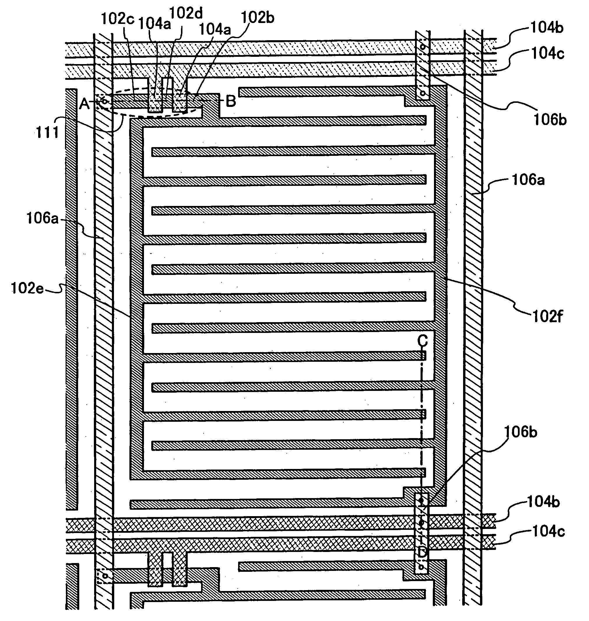
[0188] A pixel portion of a display panel of Embodiment Mode 1 of the present invention is formed over a first substrate. The pixel portion includes a plurality of wirings (hereinafter referred to as signal lines) that are supplied with a signal (hereinafter referred to as a video signal) for expressing a gray scale and a plurality of wirings (hereinafter referred to as scan lines) that selects a pixel to which the video signal is written.

[0189] In the pixel portion, a plurality of pixels are arranged in matrix corresponding to the scan lines and the signal lines. Each pixel is connected to any one of the scan lines and any one of the signal lines. Each pixel in...

embodiment mode 2

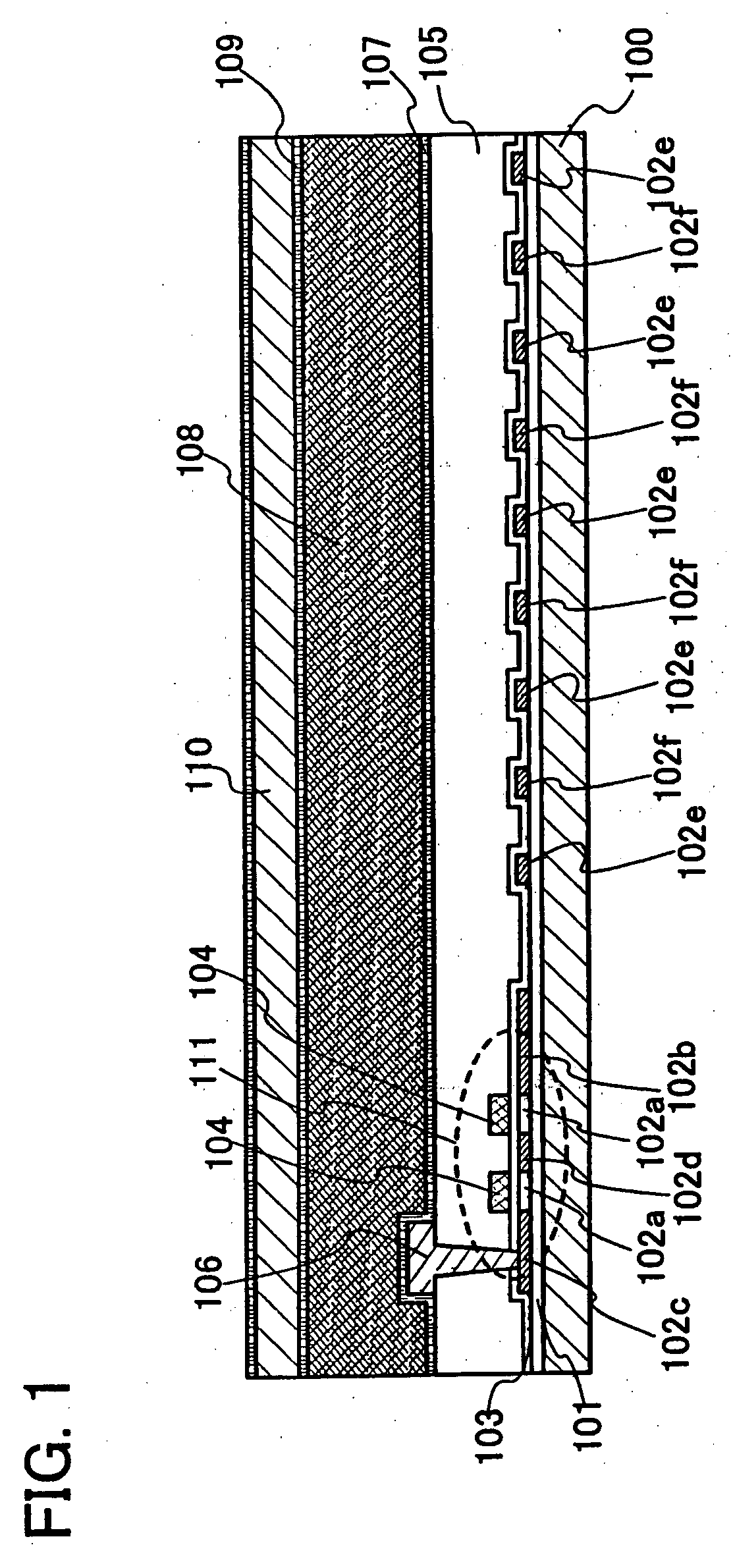
[0289] Description is made of a structure of a liquid crystal display panel of Embodiment Mode 2 of the present invention.

[0290] In the liquid crystal display panel of Embodiment Mode 2, a first insulating film is provided over a first substrate; a semiconductor layer of a transistor, and a first electrode and a second electrode of a liquid crystal element are provided over the first insulating film; a second insulating film is provided so as to cover the semiconductor layer of the transistor, and the first electrode and the second electrode of the liquid crystal element; a gate electrode is provided over the semiconductor layer of the transistor with the second insulating film interposed therebetween; a third insulating film is provided so as to cover the gate electrode and the second insulating film; a hole (contact hole) is formed in the third insulating film and the second insulating film; and a wiring formed over the third insulating film is connected to the semiconductor laye...

embodiment mode 3

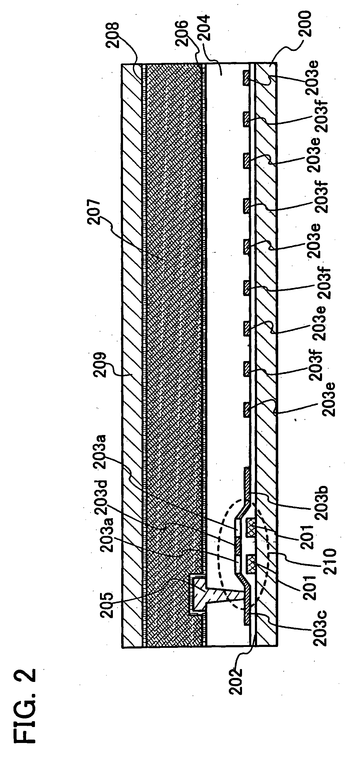
[0306] Description is made of a structure of a liquid crystal display panel of Embodiment Mode 3 of the present invention.

[0307] In the liquid crystal display panel of Embodiment Mode 3, a second electrode of a liquid crystal element is provided over a first substrate; a first insulating film is provided so as to cover the second electrode of the liquid crystal element; a semiconductor layer of a transistor, and a first electrode of the liquid crystal element are provided over the first insulating film; a second insulating film is provided so as to cover the semiconductor layer of the transistor, and the first electrode of the liquid crystal element; a gate electrode is provided over the semiconductor layer of the transistor with the second insulating film interposed therebetween; a third insulating film is provided so as to cover the gate electrode and the second insulating film; a hole (contact hole) is formed in the third insulating film and the second insulating film; and a wir...


PUM

PropertyMeasurementUnit
thicknessaaaaaaaaaa
thicknessaaaaaaaaaa
thicknessaaaaaaaaaa

Abstract

A pixel electrode or a common electrode is a light-transmissive conductive film; therefore, it is formed of ITO conventionally. Accordingly, the number of manufacturing steps and masks, and manufacturing cost have been increased. An object of the present invention is to provide a semiconductor device, a liquid crystal display device, and an electronic appliance each having a wide viewing angle, less numbers of manufacturing steps and masks, and low manufacturing cost compared with a conventional device. A semiconductor layer of a transistor, a pixel electrode, and a common electrode of a liquid crystal element are formed in the same step.

Description

BACKGROUND OF THE PRESENT INVENTION [0001] 1. Field of the Present Invention [0002] The present invention relates to a semiconductor device, a liquid crystal display device and an electronic appliance. In particular, the present invention relates to a liquid crystal display device and an electronic appliance that control molecular orientation of liquid crystal molecules by generation of an electrical field parallel to a substrate. [0003] 2. Description of the Related Art [0004] As for a liquid crystal display device, there are a vertical electrical field type in which an electrical field vertical to a substrate is applied to liquid crystal and a transverse electrical field type in which an electrical field parallel to a substrate is applied to liquid crystal. A liquid crystal display device of a transverse electrical field type is superior in a viewing angle characteristic to that of a vertical electrical field type. [0005] As a method for controlling a gray scale by generating an e...

Claims


Application Information

Patent Timeline
Patent Type & Authority Applications(United States)
IPC IPC(8): G02F1/136G02F1/1343
CPCG02B6/0051G02F1/1343G02F1/133371G02F1/133502G02F1/133524G02F1/133528G02F1/133553G02F1/133555G02F1/133603G02F1/133604G02F1/134363G02F1/13454G02F1/136213G02F1/136227G02F1/1368G02F2001/134318G02F2001/134372G02F2001/136231G02F2201/124G02F2201/50G09G3/342G09G3/3648G09G2310/024G09G2320/0252G09G2340/16H01L27/1214G02B6/0055H01L27/1225G02F1/134318G02F1/136231G02F1/134372
Inventor KIMURA, HAJIME
Owner SEMICON ENERGY LAB CO LTD
Why Eureka
Try Eureka