Liquid crystal display and method of manufacturing the same

a technology of liquid crystal display and liquid crystal, which is applied in the field of liquid crystal display, can solve the problems of low white luminance, low response speed, and time-consuming fixation of alignment, and achieve the effect of shortening the response time at a halfton

Inactive Publication Date: 2006-09-26
SHARP KK
View PDF24 Cites 92 Cited by
  • Summary
  • Abstract
  • Description
  • Claims
  • Application Information

AI Technical Summary

Benefits of technology

[0017]An object of the present invention is to provide a liquid crystal display in which an alignment orientation of a liquid crystal is regulated by using a p

Problems solved by technology

However, the conventional MVA-LCD has a defect that white luminance is low and a display is dark.
However, since the number of the protrusions or slits as the alignment regulating structural members becomes small, there arises a problem that it takes a time to fix the alignment of LC molecule even if a predetermined voltage is applied to the liquid crystal, and a response speed becomes low.
However, the polymer fixation system has some problems relating to unevenness of display when an image is displayed on a completed LCD.
First, there is a problem that unevenness of display occurs on an image display of the completed LCD due to the alignment abnormality of liquid crystal locally generated in driving the liquid crystal at the time of monomer polymerization.
Besides, there is also a problem that there occurs unevenness of display due to the abnormality of characteristics of thin film transistors (TFTs) caused by driving of liquid crystal and polymerization processing at the time of monomer polymerization.
Besides, there arises a problem that when the whole display region of the panel in the state like this is observed, the display is seen to be rough.
However, if polymerization is made in this driving state, a large fluctuation occurs in threshold

Method used


Image

  • Liquid crystal display and method of manufacturing the same
  • Liquid crystal display and method of manufacturing the same
  • Liquid crystal display and method of manufacturing the same

Examples


first embodiment

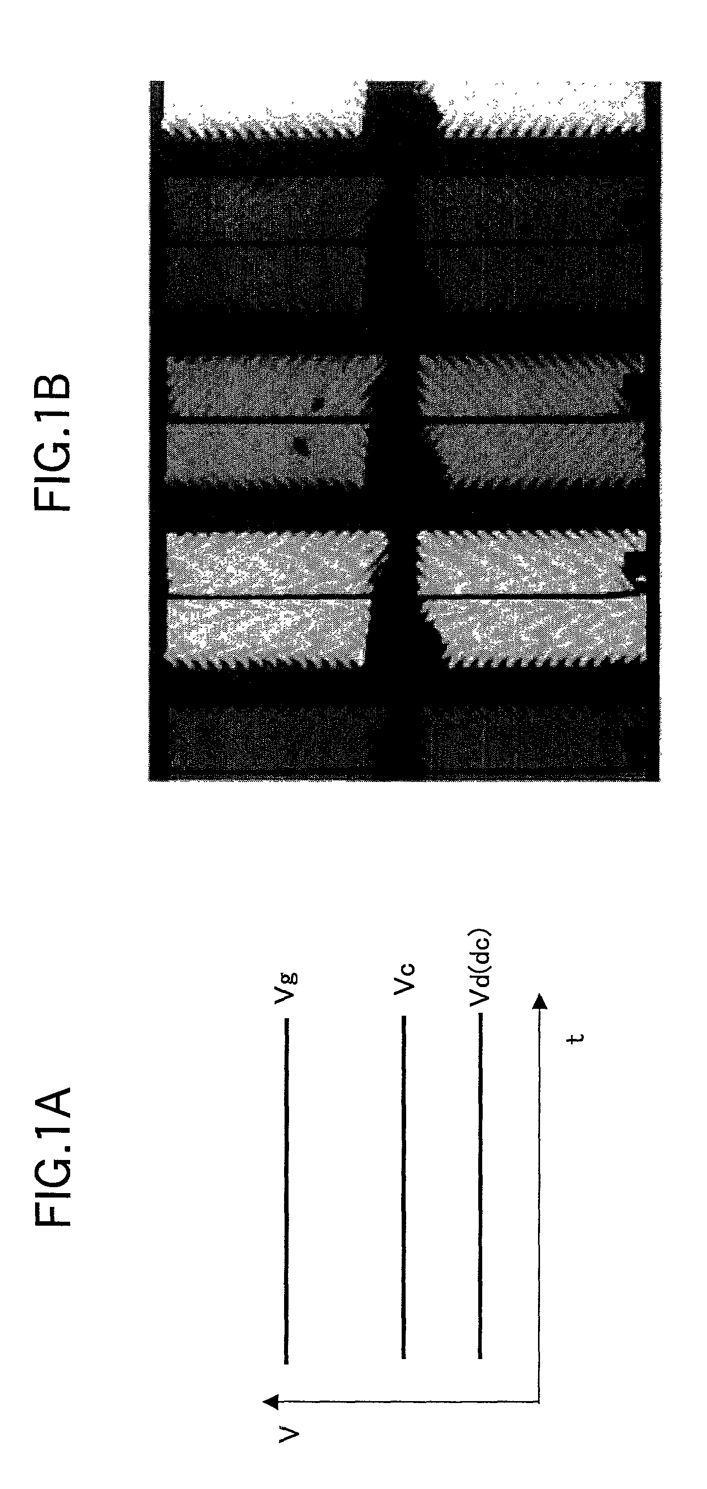
[0111]A liquid crystal display according to a first embodiment of the present invention and a method of manufacturing the same will be described with reference to FIGS. 1A to 21B. First, a first principle of the liquid crystal display and the method of manufacturing the same according to this embodiment will be described with reference to FIGS. 1A and 1B. FIG. 1A shows a liquid crystal driving method according to the first principle at the time of polymer polymerization in an MVA-LCD to which an alignment fixation processing by a polymer fixation system is performed. FIG. 1B shows a display state of the MVA-LCD in which a polymer formed by the liquid crystal driving method of the first principle shown in FIG. 1A exists in a liquid crystal layer. The n-channel type TFTs are used in this MVA-LCD.

[0112]In a polymerization step of a manufacturing stage of an LCD, the liquid crystal driving method according to the first principle is based on direct-current voltage driving, and an alterna...

example 1-1

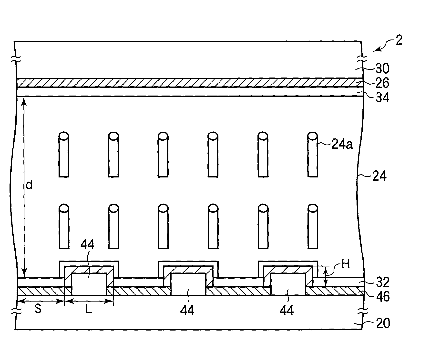
[0127]This example will be described using FIGS. 1A and 1B and FIGS. 4A and 4B again. In this example, an XGA panel (pixel pitch was 297 μm, and the number of pixels was 1024×768) having a size of 15 inches in diagonal was fabricated. The pixel structure of the panel is shown in FIGS. 4A and 4B. An n-channel TFT 16, a drain bus line 6, a gate bus line 4, and a pixel electrode formed of connection electrodes 12 and 14 and a plurality of stripe-like electrodes 8 were formed on an array substrate including a glass substrate 20. A color filter layer 28 and a common electrode 26 were formed on an opposite substrate including a glass substrate 30. A glass substrate having a thickness of 0.7 mm was used as a substrate material. The plurality of stripe-like electrodes 8 were formed to extend in four directions (upper right, lower right, upper left, lower left) from the center portion of the pixel, respectively. The electrode width of the stripe-like electrode 8 was made 3 μm, and the width ...

example 1-2

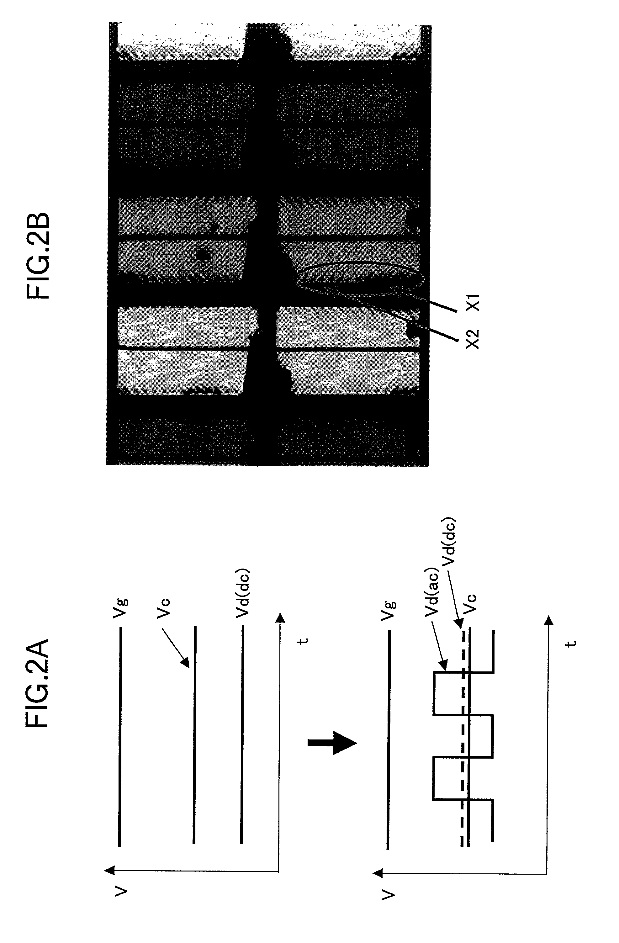
[0141]This example will be described with reference to FIGS. 2A and 2B. This example is the same as the example 1-1 except for the following requirements. The driving voltage was applied to the liquid crystal layer 24 under a voltage application condition 2 subsequently to a voltage application condition 1 mentioned below, and the driving voltage was further applied under a voltage application condition 3, and light irradiation to the liquid crystal layer 24 was performed at the stage of the voltage application condition 3;[0142]voltage application condition 1: Vg=33 V, Vc=Vd (dc)=13 V,[0143]voltage application condition 2: Vg=33 V, Vc=20 V, Vd (dc)=13 V, and[0144]voltage application condition 3: Vg=33 V, Vc=Vd (dc)=13 V, Vd (ac)=7 V (30 Hz).

[0145]After the liquid crystal driving similar to the example 1-1, while the common voltage Vc was made to gradually approach the value of the data voltage Vd (dc), the amplitude of the data voltage Vd (ac) was gradually increased. By this, in t...


PUM


Abstract

The invention has an object to provide a liquid crystal display in which a wide angle of view is obtained and a response time at a halftone can be shortened by regulating an alignment orientation of a liquid crystal by the use of a polymer fixation system in which a liquid crystal layer containing a polymerizable component is sealed between substrates, and the polymerizable component is polymerized while a voltage is applied to the liquid crystal layer to fix a liquid crystal alignment. A liquid crystal layer containing a polymer for regulating a pretilt angle of a liquid crystal molecule and a tilt direction at a time of driving is sealed between two substrates arranged opposite to each other. A plurality of stripe-like electrode patterns in which a pattern width is formed to be wider than a width of a space, are arranged so that the liquid crystal molecule is aligned in a longitudinal direction of the pattern when the polymer is formed by solidifying a polymerizable component mixed in the liquid crystal layer while a voltage is applied to the liquid crystal layer.

Description

BACKGROUND OF THE INVENTION[0001]1. Field of the Invention[0002]The present invention relates to a liquid crystal display in which a liquid crystal layer containing a polymerizable component (monomer or oligomer), which is polymerized by light or heat, is sealed between substrates, and the polymerizable component is polymerized while a voltage is applied to the liquid crystal layer to fix a tilting direction of a liquid crystal molecules, and a method of manufacturing the same.[0003]Besides, the present invention relates to a liquid crystal display of a VA (VerticallyAligned) mode in which a liquid crystal having a negative dielectric anisotropy is vertically aligned, and a method of manufacturing the same.[0004]2. Description of the Related Art[0005]A multi-domain vertical alignment mode liquid crystal display (hereinafter abbreviated to an MVA-LCD) is known in which a liquid crystal having a negative dielectric anisotropy is vertically aligned and a bank (linear protrusion) or a c...

Claims


Application Information

Patent Timeline
IPC IPC(8): G02F1/1343G02F1/1333G02F1/1337G02F1/1339G02F1/1362G02F1/1368G02F1/139
CPCG02F1/133788G02F1/133707G02F1/134363G02F1/1393G02F1/1362G02F1/1337
Inventor HANAOKA, KAZUTAKA
Owner SHARP KK
Why Eureka
Try Eureka