Display device, manufacturing method thereof, and television set

a technology of a display device and a manufacturing method, applied in the field of display devices, can solve the problems blurred images, and limitation of viewing angle characteristics, and achieve the effects of high speed operation, low resistivity, and high mobility

Inactive Publication Date: 2009-07-21
SEMICON ENERGY LAB CO LTD
View PDF18 Cites 89 Cited by
  • Summary
  • Abstract
  • Description
  • Claims
  • Application Information

AI Technical Summary

Benefits of technology

[0011]The invention is made in view of the aforementioned circumstances, and it is a primary object of the invention to provide a manufacturing method of a display device having TFTs capable of high-speed operation, which has few variations of threshold voltage and requires a small number of photomasks. It is another object of the invention to provide a manufacturing method of a display device having an excellent switching property and high image contrast.
[0013]According to the invention, an inversely staggered thin film transistor is manufactured by forming a crystalline semiconductor film by doping a catalytic element into an amorphous semiconductor film and heating it, and then removing the catalytic element from the crystalline semiconductor film. In addition, according to the invention, a gate electrode layer of a thin film transistor and a pixel electrode layer are formed using the same steps and material, thereby simpler manufacturing steps are achieved as well as the reduction of waste of materials. In addition, the display device of the invention has a liquid crystal display element using a liquid crystal material or a light-emitting element (EL element) as a display element, which may thus be called a liquid crystal display device, a light-emitting display device, or an EL display device.
[0027]According to the invention, an inversely staggered thin film transistor having a crystalline semiconductor film can be formed. Therefore, a TFT can be formed with a small number of photomasks. In addition, since the TFT of the invention is formed using a crystalline semiconductor film, it exhibits higher mobility as compared to an inversely staggered TFT formed using an amorphous semiconductor film. A source region and a drain region of the TFT are doped with metal elements which promote crystallization in addition to p-type impurity elements (acceptor elements) or n-type impurity elements (donor elements). Therefore, the source region and the drain region can be formed to have low resistivity. As a result, a display device capable of high-speed operation can be manufactured. Typically, a display device such as an OCB-mode display device can be manufactured, which exhibits high response while being capable of displaying images with a wide viewing angle.
[0028]In addition, in comparison with a thin film transistor formed using an amorphous semiconductor film, variations of threshold voltage hardly occur, resulting in the decrease in variations of the TFT characteristics. Therefore, display unevenness can be decreased, and a highly reliable display device can thus be manufactured.
[0029]Further, metal elements which are mixed into the semiconductor film during the film deposition are removed by a gettering step; therefore, off current can be decreased. By using such a TFT as a switching element of the display device, image contrast can be enhanced.
[0030]Further, according to the invention, waste of materials can be reduced, resulting in cost saving. Thus, a high-performance and highly reliable display device can be manufactured with high yield.

Problems solved by technology

Meanwhile, in the conventional liquid crystal television set, there has been a defect in that images are blurred due to the limitation of the viewing angle characteristics, limitation of the high speed operation with liquid crystal materials, and the like.
Therefore, in the display device using such a TFT formed of an amorphous semiconductor film for switching of the pixel, luminance unevenness occurs.
Such a phenomenon is recognized more often in a large-screen television set having an opposite angle of 30 inches or more (typically, 40 inches or more), which thus poses a serious problem regarding the degradation in image quality.
However, the TFT using an amorphous semiconductor film has a limitation in operation speed.
For example, it is difficult to realize a liquid crystal display device in the OCB mode.

Method used


Image

  • Display device, manufacturing method thereof, and television set
  • Display device, manufacturing method thereof, and television set
  • Display device, manufacturing method thereof, and television set

Examples


embodiment mode 1

[0102]In this embodiment mode, description is made in detail. Although the invention will be fully described by way of examples with reference to the accompanying drawings, it is to be understood that various changes and modifications will be apparent to those skilled in the art. Therefore, unless otherwise such changes and modifications depart from the scope of the invention, they should be constructed as being included therein. Note that common portions or portions having a common function in the structure of the invention are denoted by common reference numerals in all the drawings, and therefore, the description thereof is made only once.

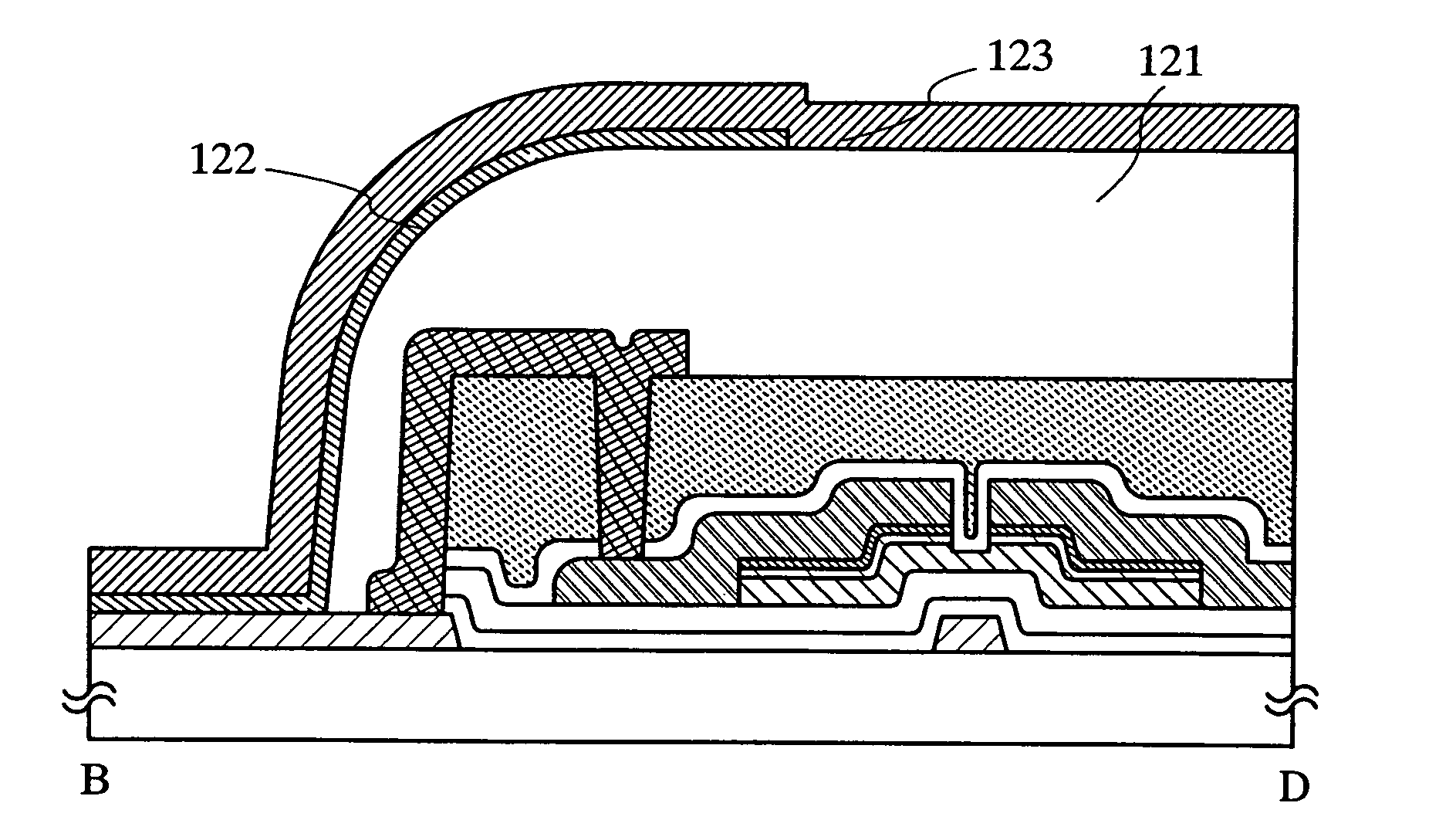
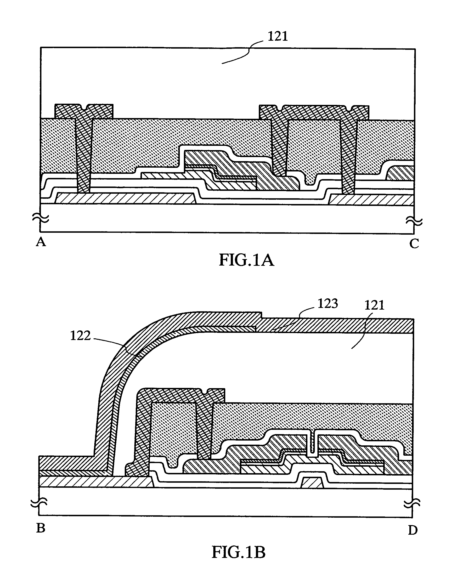
[0103]FIG. 29A is a top view illustrating the structure of a display panel in accordance with the invention. Over a substrate 2700 having an insulating surface, a pixel portion 2701 having a matrix arrangement of pixels 2702, a scan line side input terminal 2703, and a signal line side input terminal 2704 are formed. The number of the pixels may...

embodiment mode 2

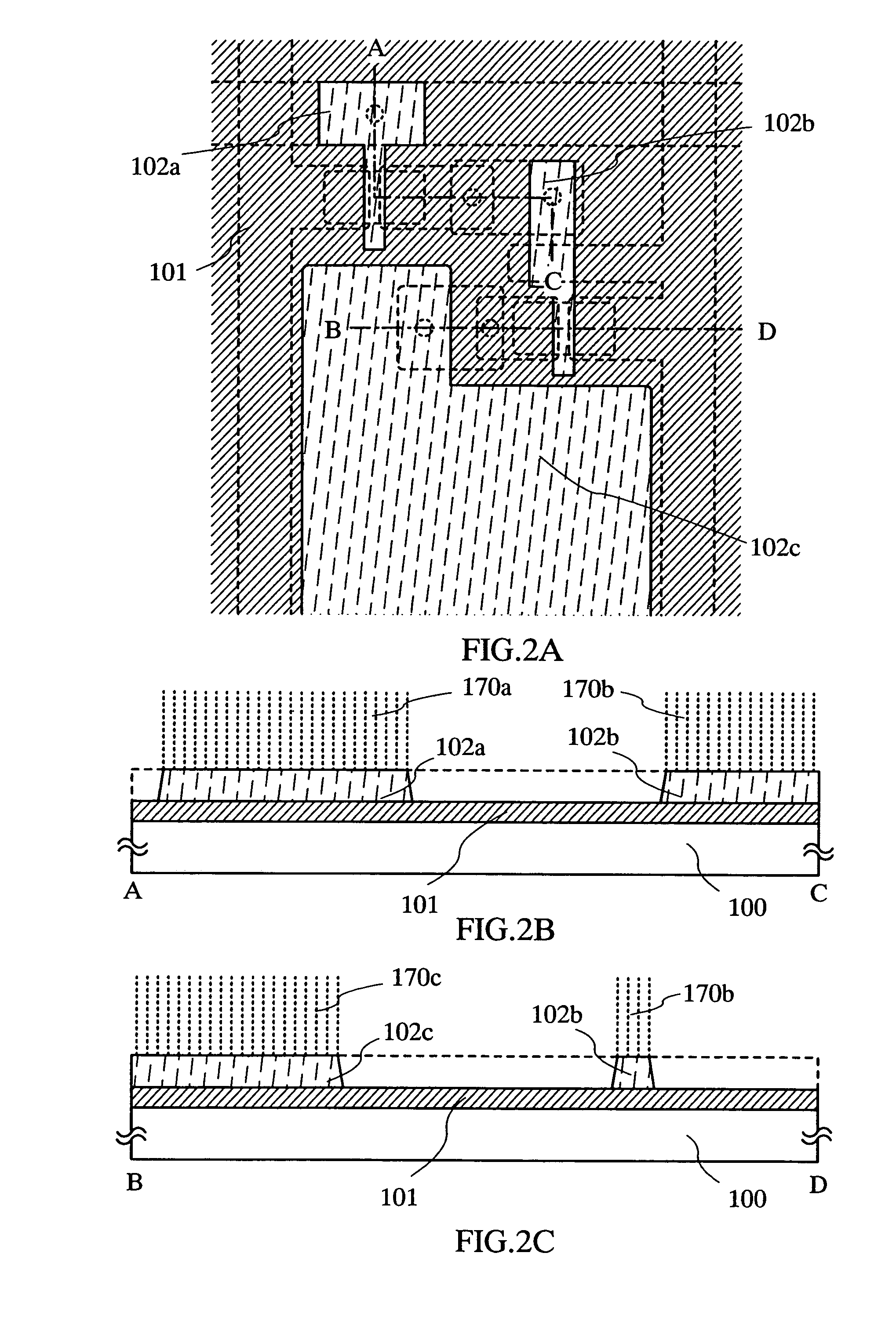
[0190]One embodiment mode of the invention will be described with reference to FIGS. 10A to 10F. This embodiment mode is different from Embodiment 1 in the gettering steps of a crystalline semiconductor film. Therefore, common portions or portions having a common function will be described in no more detail.

[0191]Over a substrate 400, a gate electrode layer 401 is formed, which is covered with gate insulating layers 402a and 402b. Over the gate insulating layer 402b, an amorphous semiconductor film 403 and a metal film 404 are formed (see FIG. 10A). Then, the amorphous semiconductor film 403 is crystallized by thermal treatment to obtain a crystalline semiconductor film 405(see FIG. 10B).

[0192]In this embodiment mode, a semiconductor layer 421 containing rare gas elements as impurity elements is formed as a gettering layer for gettering metal elements for promoting crystallization, which are contained in the crystalline semiconductor film 405. The rare gas elements may be helium, ar...

embodiment mode 3

[0197]One embodiment mode of the invention will be described with reference to FIGS. 11A to 11D. This embodiment mode is an example in which two kinds of thin film transistors: an n-channel thin film transistor and a p-channel thin film transistor are manufactured. Therefore, common portions or portions having a common function will be described in no more detail.

[0198]Over a substrate 430, gate electrode layers 431a and 431b, and gate insulating layers 433a and 433b are formed. Over the gate insulating layer 433b, an amorphous semiconductor film is formed, to which metal elements are doped. Then, the amorphous semiconductor is crystallized by thermal treatment to obtain a crystalline semiconductor film. Over the crystalline semiconductor film, an n-type semiconductor film 435 is formed and heated (see FIG. 11A).

[0199]By the thermal treatment, metal elements contained in the crystalline semiconductor film are gettered, which travel in the direction of arrows to be trapped into the n...


PUM


Abstract

A manufacturing method of a display device having TFTs capable of high-speed operation with few variations of threshold voltage is provided, in which materials are used with high efficiency and a small number of photomasks is required. The display device of the invention comprises a gate electrode layer and a pixel electrode layer formed over an insulating surface, a gate insulating layer formed over the gate electrode layer, a crystalline semiconductor layer formed over the gate insulating layer, a semiconductor layer having one conductivity type formed in contact with the crystalline semiconductor layer, a source electrode layer and a drain electrode layer formed in contact with the semiconductor layer having one conductivity type, an insulating later formed over the source electrode layer, the drain electrode layer, and the pixel electrode layer, a first opening formed in the insulating layer to reach the source electrode layer or the drain electrode layer, a second opening formed in the gate insulating layer and the insulating layer to reach the pixel electrode layer, and a wiring layer formed in the first opening and the second opening to electrically connect the source electrode layer or the drain electrode layer to the pixel electrode layer.

Description

BACKGROUND OF THE INVENTION[0001]1. Field of the Invention[0002]The present invention relates to a display device and a manufacturing method thereof. In addition, the invention relates to a television set using the display device.[0003]2. Description of the Related Art[0004]In recent years, a flat panel display (FPD) is attracting attention as an alternative display device for a conventional CRT display device. In particular, development of a large-screen television set mounted with a large display panel which is driven with an active matrix method is the primary task for panel manufacturers.[0005]In the conventional display device, a semiconductor element for driving each pixel is formed of a thin film transistor (hereinafter also referred to as a TFT) which uses amorphous silicon as its active layer (see Patent Document 1).[0006]Meanwhile, in the conventional liquid crystal television set, there has been a defect in that images are blurred due to the limitation of the viewing angl...

Claims


Application Information

Patent Timeline
Patent Type & Authority Patents(United States)
IPC IPC(8): H01L27/14
CPCG02F1/1368H01L21/2022H01L21/2026H01L27/12H01L27/1292H01L27/3262H01L27/124H01L27/1277H01L27/3248G02F2202/104H01L27/3246H01L27/3276H01L51/56H01L21/02576H01L21/02422H01L21/02488H01L21/02496H01L21/02505H01L21/0242H01L21/02672H01L21/02581H01L21/0262H01L21/02425H01L21/02491H01L21/02532H01L21/0245H01L21/02579H01L21/02381H10K59/123H10K59/1213H10K59/122H10K59/131H10K71/00G02F1/136H01L21/02667
Inventor YAMAZAKI, SHUNPEISHOJI, HIRONOBUMAEKAWA, SHINJINAKAMURA, OSAMUHONDA, TATSUYAFUJII, GENSUZUKI, YUKIEKAWAMATA, IKUKO
Owner SEMICON ENERGY LAB CO LTD
Why Eureka
Try Eureka