Chiplets with connection posts

a technology of connection posts and chiplets, applied in the direction of final product manufacturing, sustainable manufacturing/processing, semiconductor/solid-state device details, etc., can solve the problems of wasting material and processing costs, reducing the performance of above-the-line integrated circuits, and reducing the performance of other integrated circuits. , to achieve the effect of reducing process steps, simple and inexpensive electrical interconnection process

Active Publication Date: 2017-02-16
X DISPLAY CO TECH LTD
View PDF47 Cites 110 Cited by
  • Summary
  • Abstract
  • Description
  • Claims
  • Application Information

AI Technical Summary

Benefits of technology

[0017]Because the components can be made using integrated circuit photolithographic techniques having a relatively high resolution and cost and the destination substrate, for example a printed circuit board, can be made using printed circuit board techniques having a relatively low resolution and cost, the backplane contact pads on the destination substrate can be much larger than the connection posts or electrical contacts on the component, facilitating the use of multiple connection posts with a common backplane contact pads, reducing electrical faults, and reducing manufacturing costs.
[0098]The present invention provides structures and methods that enable the construction of electrical interconnections between small integrated circuits that are transfer printed on a destination substrate. The electrical interconnection process is simple and inexpensive requiring fewer process steps than known alternative methods.

Problems solved by technology

The above techniques have some limitations.
Despite processing methods used to improve the performance of thin-film transistors, such transistors may provide performance that is lower than the performance of other integrated circuits formed in mono-crystalline semiconductor material.
Semiconductor material and active components can be provided only on portions of the substrate, leading to wasted material and processing costs.
The choice of substrate materials can also be limited by the processing steps necessary to process the semiconductor material and the photo-lithographic steps used to pattern the active components.
For example, plastic substrates have a limited chemical and heat tolerance and do not readily survive photo-lithographic processing.
Furthermore, the manufacturing equipment used to process large substrates with thin-film circuitry is relatively expensive.
However, such substrate materials can be more expensive or difficult to process.
However, these techniques may be limited in the size of the integrated circuits that can be placed.
While this approach can provide substrates with the same performance as integrated circuits, the size of such substrates may be limited, for example, to a 12-inch diameter circle, and the wafers are relatively expensive compared to other substrate materials such as glass, polymer, or quartz.
However, the bonding technique and the processing equipment for the substrates to form the thin-film active components on large substrates can be relatively expensive.
This method may require etching a significant quantity of material, and may risk damaging the exposed TFT array.
These methods, however, may require the patterned deposition of adhesive on the object(s) or on the second substrate.
Moreover, the laser beam that irradiates the object may need to be shaped to match the shape of the object, and the laser abrasion can damage the object to be transferred.
Furthermore, the adhesive cure takes time, which may reduce the throughput of the manufacturing system.
This process is expensive and requires a number of manufacturing steps.
Moreover, the topographical structure of the small integrated circuits over the destination substrate renders the electrical connections problematic.
For example it can be difficult to form a continuous conductor from the destination substrate to the small integrated circuit because of the differences in height over the surface between the small integrated circuits and the destination substrate.

Method used


Image

  • Chiplets with connection posts
  • Chiplets with connection posts
  • Chiplets with connection posts

Examples


Embodiment Construction

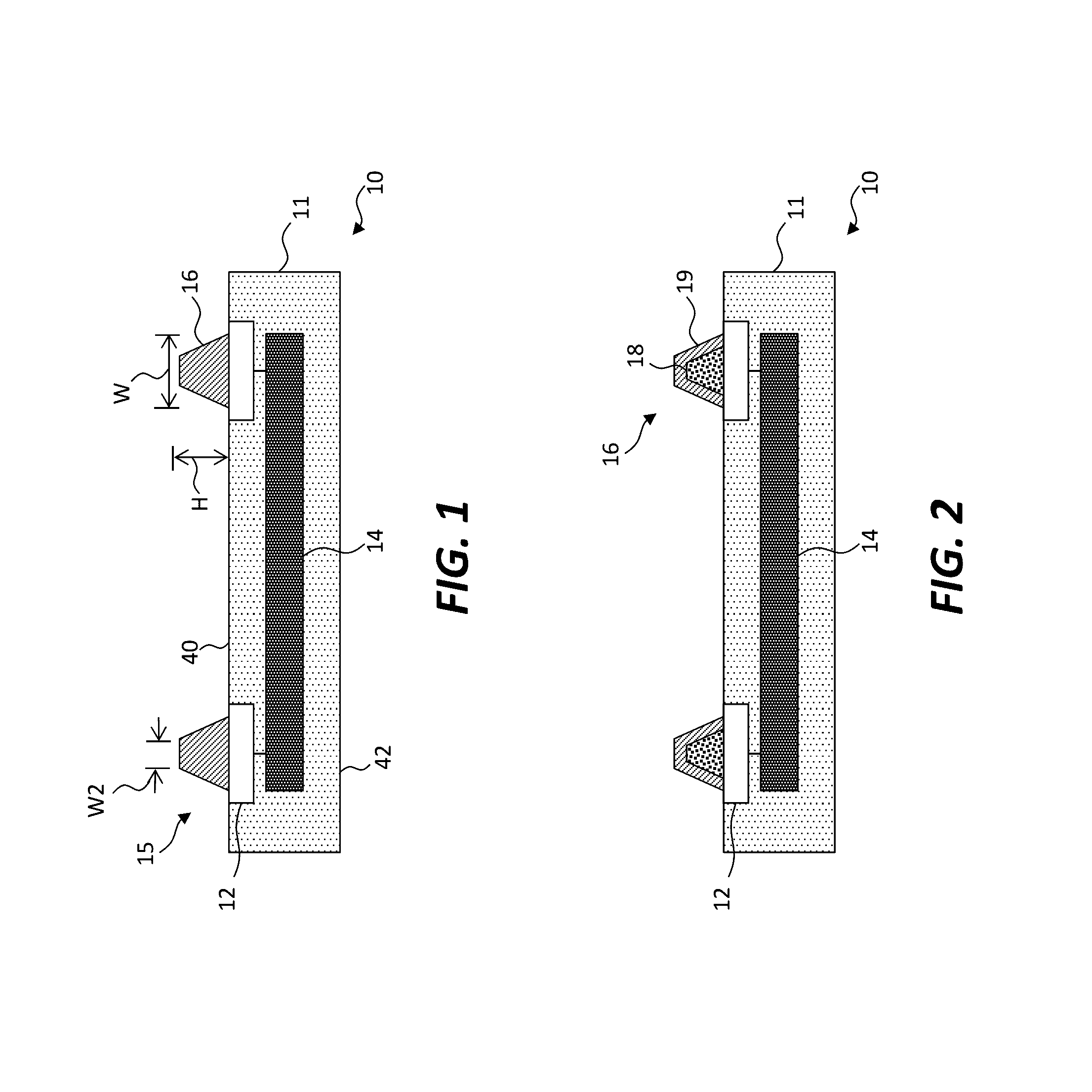
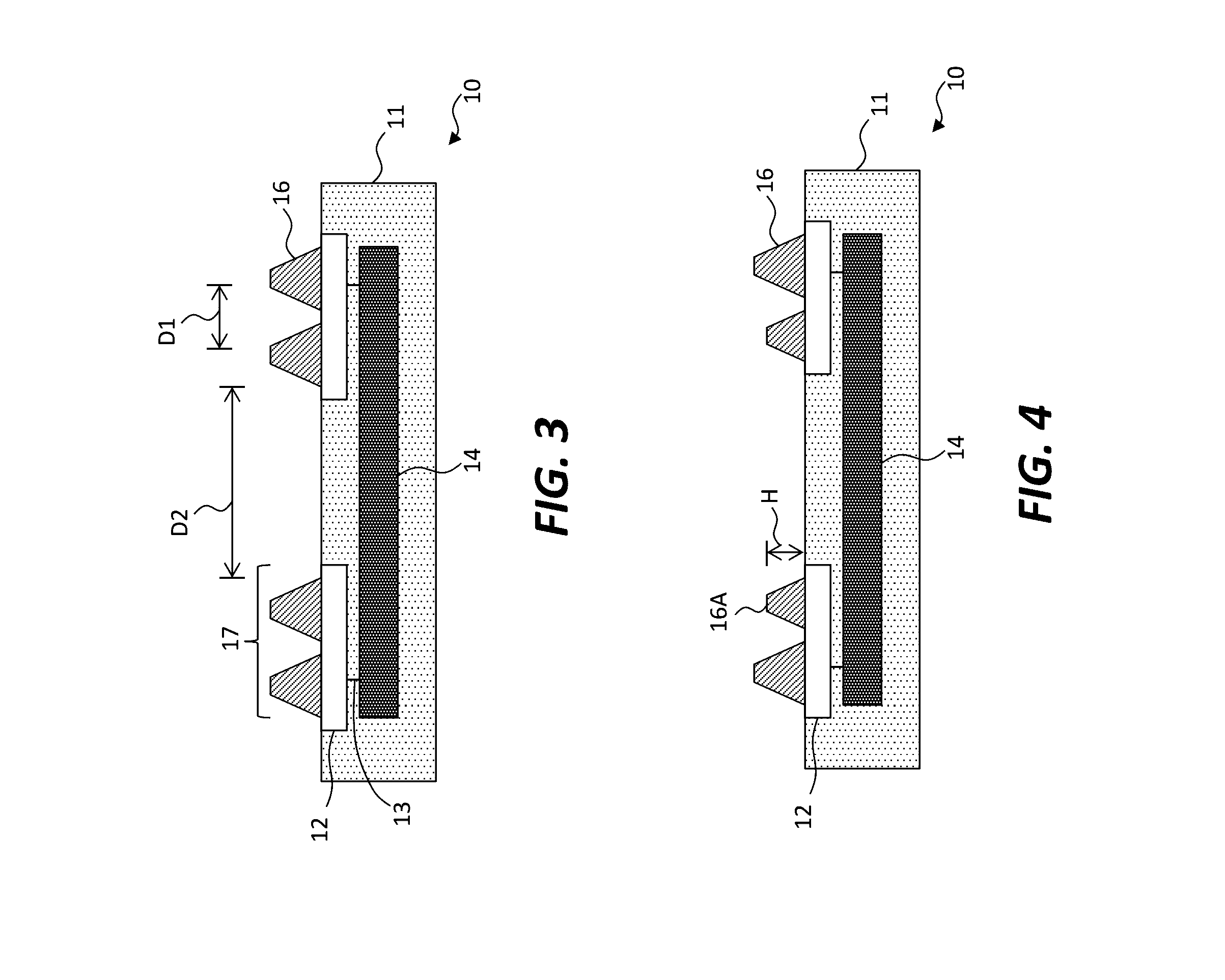
[0116]The present invention provides a structure and method for electrically connecting relatively small electrical components such as integrated circuit chiplets to a relatively large destination substrate in an efficient and cost-effective way. Referring to the cross section of FIG. 1, in an embodiment of the present invention, a component 10 includes a plurality of electrical connections 15 on a process side 40 opposed to a back side 42 of the component 10. Each electrical connection 15 includes an electrically conductive connection post 16 protruding from the process side 40. The electrical connection 15 can also include a component contact pad 12 on which the connection post 16 is disposed and to which the connection post 16 is electrically connected.

[0117]The component 10 can be an active component, for example including one or more active elements such as electronic transistors or diodes or light-emitting diodes and photodiodes that produce an electrical current in response t...


PUM


Abstract

A component includes a plurality of electrical connections on a process side opposed to a back side of the component. Each electrical connection includes an electrically conductive multi-layer connection post protruding from the process side. A printed structure includes a destination substrate and one or more components. The destination substrate has two or more electrical contacts and each connection post is in contact with, extends into, or extends through an electrical contact of the destination substrate to electrically connect the electrical contacts to the connection posts. The connection posts or electrical contacts are deformed. Two or more connection posts can be electrically connected to a common electrical contact.

Description

CROSS REFERENCE TO RELATED APPLICATION[0001]Reference is made to U.S. Pat. No. 8,889,485, entitled Methods for Surface Attachment of Flipped Active Components by Christopher Bower, the disclosure of which is incorporated herein by reference in its entirety.FIELD OF THE INVENTION[0002]The present invention relates to structures and methods for electrically interconnecting chiplets to backplane contact pads using micro transfer printing.BACKGROUND OF THE INVENTION[0003]Substrates with electronically active components distributed over the extent of the substrate may be used in a variety of electronic systems, for example, flat-panel imaging devices such as flat-panel liquid crystal or organic light emitting diode (OLED) display devices and in flat-panel solar cells. A variety of methods may be used to distribute electronically active circuits over substrates, including forming the electronically active circuits on a substrate and forming the components on separate substrates and placin...

Claims


Application Information

Patent Timeline
Patent Type & Authority Applications(United States)
IPC IPC(8): H05K1/11H01L23/00
CPCH05K1/112H05K2201/09409H01L24/14H01L24/08H01L24/11H01L2224/13023H01L2224/1357H01L2224/1403H01L2224/1412H01L2224/16227H01L2224/1624H01L2224/17107H01L2224/11466H05K2201/09472H01L24/13H05K3/305H05K3/3436H05K2201/0979H05K2201/10143H01L2924/12041H01L2924/12044H01L2924/12043H01L2924/1304H01L2924/14H01L2224/1411H01L24/81H01L2224/0401H01L24/05H01L2224/81005H01L24/95H01L2224/95001H01L2224/81191H01L2224/81801H01L2224/81815H01L2224/81193H01L2224/1418H01L24/06H01L24/17Y02P70/50H01L24/98H01L2224/11612H01L2224/1161H01L2224/1182H01L2224/131H01L2224/136H01L2924/00012H01L2924/01014H01L2224/13017H01L2224/1144
Inventor PREVATTE, CARLBOWER, CHRISTOPHERCOK, RONALD S.MEITL, MATTHEW
Owner X DISPLAY CO TECH LTD
Why Eureka
Try Eureka