Apparatus for manufacturing flat panel display devices

a technology for flat panel display and display devices, which is applied in the direction of manufacturing tools, optical radiation measurement, instruments, etc., can solve the problems of non-uniform crystallinity of silicon films, difficult to shape the intensity distribution of laser beams to a distribution, and inability to obtain silicon films of desired performance, etc., to achieve uniform crystallinity, improve the quality of silicon films, and high yield

Active Publication Date: 2007-03-20
JAPAN DISPLAY INC +1
View PDF8 Cites 11 Cited by
  • Summary
  • Abstract
  • Description
  • Claims
  • Application Information

AI Technical Summary

Benefits of technology

[0018]An object of the present invention is to solve the aforementioned problems, that is, to provide a flat panel display deice manufacturing apparatus in which a silicon crystal film of uniform performance can be formed stably while the spatial intensity distribution, beam diameter and optical axis of a laser beam can be always kept in a desired state when the apparatus operates for a long time. As a result, the object of the invention is to improve the yield in a process for manufacturing flat panel display devices.
[0020]According to the flat panel display device manufacturing apparatus of the invention for achieving the aforementioned method, the silicon thin film can be stably irradiated with the laser beam having a desired spatial intensity distribution, so that silicon thin films having uniform crystallinity can be formed in high yield.
[0021]According to the flat panel display device manufacturing apparatus of the invention, when a solid-state laser beam of high coherence and a solid-state laser beam shaping optical element very sensitive to irregular change in the intensity distribution, optical axis and beam diameter of the incident laser beam are used for improving the quality of a silicon film while the intensity distribution of the laser beam incident on the laser beam shaping optical element or the laser beam shaped by the laser beam shaping optical element is always monitored, the number of bad panels can be reduced while the uniformity of the laser beam applied on the silicon film can be kept high.

Problems solved by technology

Accordingly, if a silicon thin film is irradiated with a laser beam having such a Gaussian function type spatial intensity distribution to improve the quality of the silicon thin film by laser irradiation, a silicon film non-uniform in crystallinity is generated because the melting duration in the central portion of the irradiated region is different from the melting duration in the end portion of the irradiated region.
As a result, it is impossible to obtain a silicon film of desired performance.
Accordingly, if beam splitting type laser beam shaping means such as a multi-lens array is applied as represented by an excimer laser beam shaping optical system used in low-temperature polysilicon mass production technology at present, it is very difficult to shape the intensity distribution of the laser beam to a distribution suitable for irradiation of a silicon film because the distribution is affected by diffraction occurring at the time of splitting of the laser beam and interference occurring at the time of synthesizing the split laser beam components.
Secondly, the position of the laser beam incident on the laser beam shaping optical element must coincide with the designed position.
The fact that the intensity distribution of the laser beam applied on the silicon film comes out of the desired distribution means the fact that the crystallinity of the formed silicon film becomes non-uniform.

Method used


Image

  • Apparatus for manufacturing flat panel display devices
  • Apparatus for manufacturing flat panel display devices
  • Apparatus for manufacturing flat panel display devices

Examples


embodiment 1

[Embodiment 1]

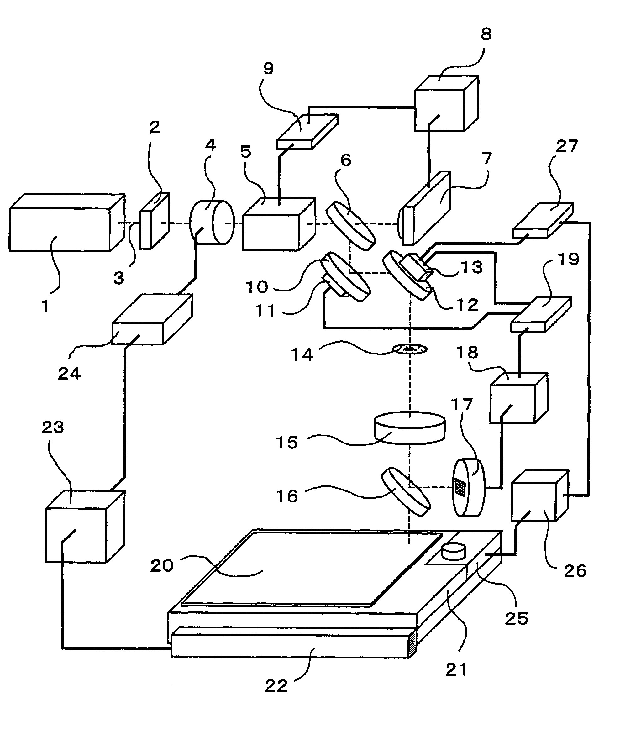
[0040]FIG. 1 is a perspective view showing the schematic configuration of a laser annealing apparatus as Embodiment 1 of an apparatus for manufacturing flat panel display devices according to the invention. The laser annealing apparatus comprises a laser diode (LD)-pumped continuous-wave (CW) solid-state laser 1, a neutral-density (ND) filter 2, an electro-optical (EO) modulator 4, a spatial filter and beam expander 5, a laser beam splitting system 6, a beam profiler 7, a signal processing unit 8, a driver 9, optical axis alignment mirrors 10 and 12, an iris 14, a laser beam shaping optical element 15, a laser beam splitting system 16, a laser beam spatial intensity distribution detecting system 17, a signal processing unit 18, a driver 19, a glass substrate 20, a stage 21, a linear encoder (also referred to as linear scale) 22, a controller 23, a driver 24, a beam profiler 25, a signal processor 26, and a driver 27. The LD-pumped CW solid-state laser 1 is used as a la...

embodiment 2

[Embodiment 2]

[0075]Next, a mechanism for detecting the displacement in the position of the laser beam incident on the laser beam shaping optical element and correcting the incidence position to a predetermined incidence position will be described as Embodiment 2 of the invention. The outline and configuration of this embodiment will be described first with reference to FIG. 10. The correcting method using the incidence position correcting mechanism according to this embodiment will be then described in detail with reference to FIGS. 11 to 15.

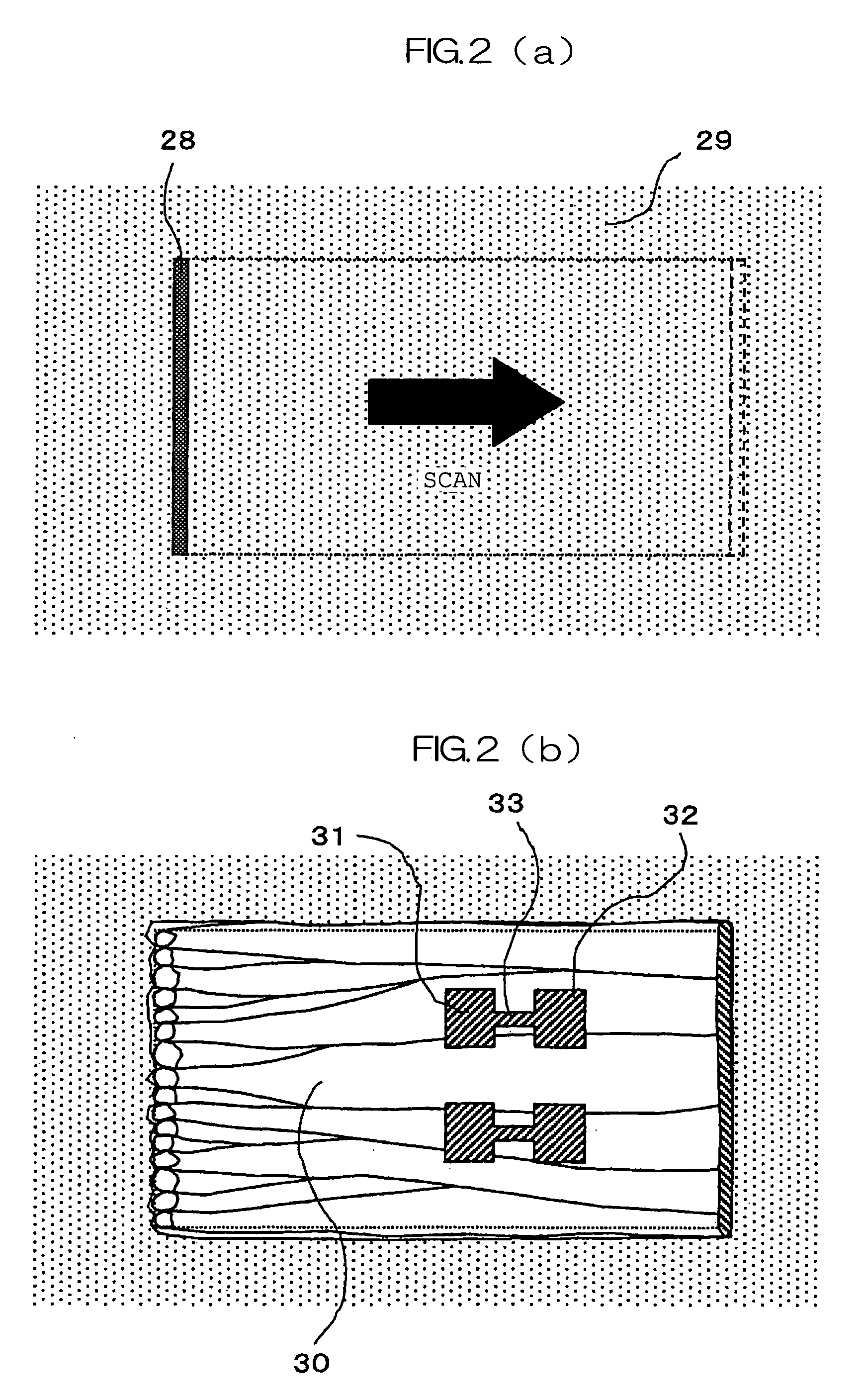
[0076]FIG. 10 is a perspective view for explaining an example of a process for correcting the position of the laser beam incident on the laser beam shaping optical element in Embodiment 2 of the apparatus for manufacturing flat panel display devices according to the invention. FIG. 10 shows the schematic configuration of a laser beam irradiation position control system and an irradiation optical system corresponding to this embodiment in the fl...


PUM

PropertyMeasurementUnit
diameteraaaaaaaaaa
crystallinityaaaaaaaaaa
speedaaaaaaaaaa

Abstract

A mechanism for always measuring the spatial intensity distribution of a laser beam and displacement of the optical axis of the laser beam is provided so that a measured signal is processed when the laser beam incident on a laser beam shaping optical element is out of a predetermined condition. The shape, diameter and incidence position of the laser beam incident on the laser beam shaping optical element are always kept in the predetermined condition by a spatial filter disposed at the position of a focal point of lenses forming a beam expander disposed in the optical axis, on the basis of a result of the signal processing.In this manner, silicon thin films uniform in crystallinity can be formed stably with a high yield on an insulating substrate which forms display panels of flat panel display devices.

Description

BACKGROUND OF THE INVENTION[0001]The present invention relates to an apparatus for manufacturing flat panel display devices composed of thin film transistors formed in such a manner that a semiconductor film formed on an insulating substrate is irradiated with a laser beam to attain improvement of film quality or magnification or pseudo single crystallization of crystal grains.[0002]At present, a liquid crystal display device or an organic electroluminescence (EL) display device forms an image by switching of thin film transistors formed from an amorphous silicon film on a substrate such as a glass substrate or a fused quartz substrate. If a driver circuit for driving the pixel transistors can be formed together with the transistors on the substrate, there is some expectation that reduction in production cost and improvement in reliability will be made remarkably.[0003]In the present situation, the crystallinity of a silicon thin film used for forming active layers of such transisto...

Claims


Application Information

Patent Timeline
Patent Type & Authority Patents(United States)
IPC IPC(8): G01N21/00B23K26/06G01J1/00G02F1/1345B23K26/073G02F1/136G02F1/1368G09G3/36G09G3/38H01L21/00H01L21/20H01L21/268H01L21/324H01L21/336H01L21/84H01L29/786
CPCB23K26/073B23K26/422H01L27/14625B23K26/702
Inventor YAZAKI, AKIOHONGO, MIKIOHATANO, MUTSUKONODA, TAKESHI
Owner JAPAN DISPLAY INC
Why Eureka
Try Eureka