
Circuit, system and method for encoding data to be stored on a non-volatile memory array

a non-volatile memory array and data technology, applied in the field of non-volatile memory (“ nvm”) devices, can solve the problem of discovering errors but doing nothing to correct them

Active Publication Date: 2007-03-27
SAMSUNG ELECTRONICS CO LTD
View PDF2 Cites 156 Cited by
  • Summary
  • Abstract
  • Description
  • Claims
  • Application Information

AI Technical Summary

Benefits of technology

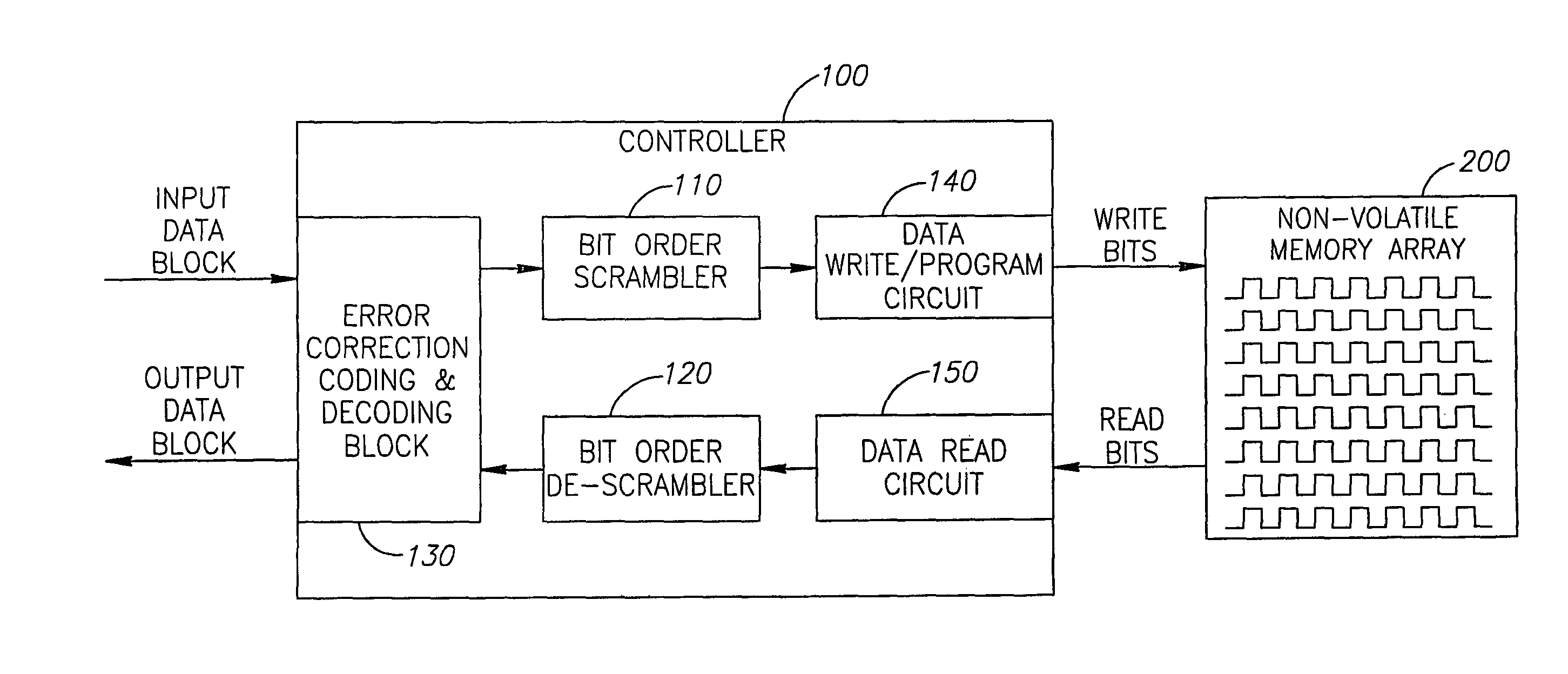
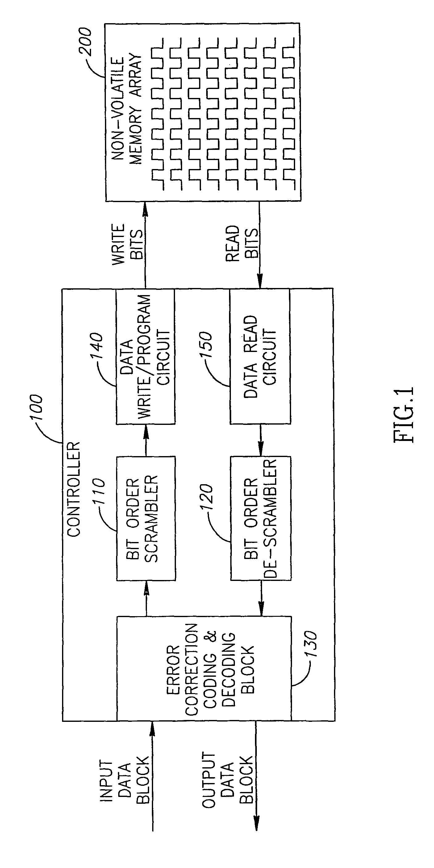
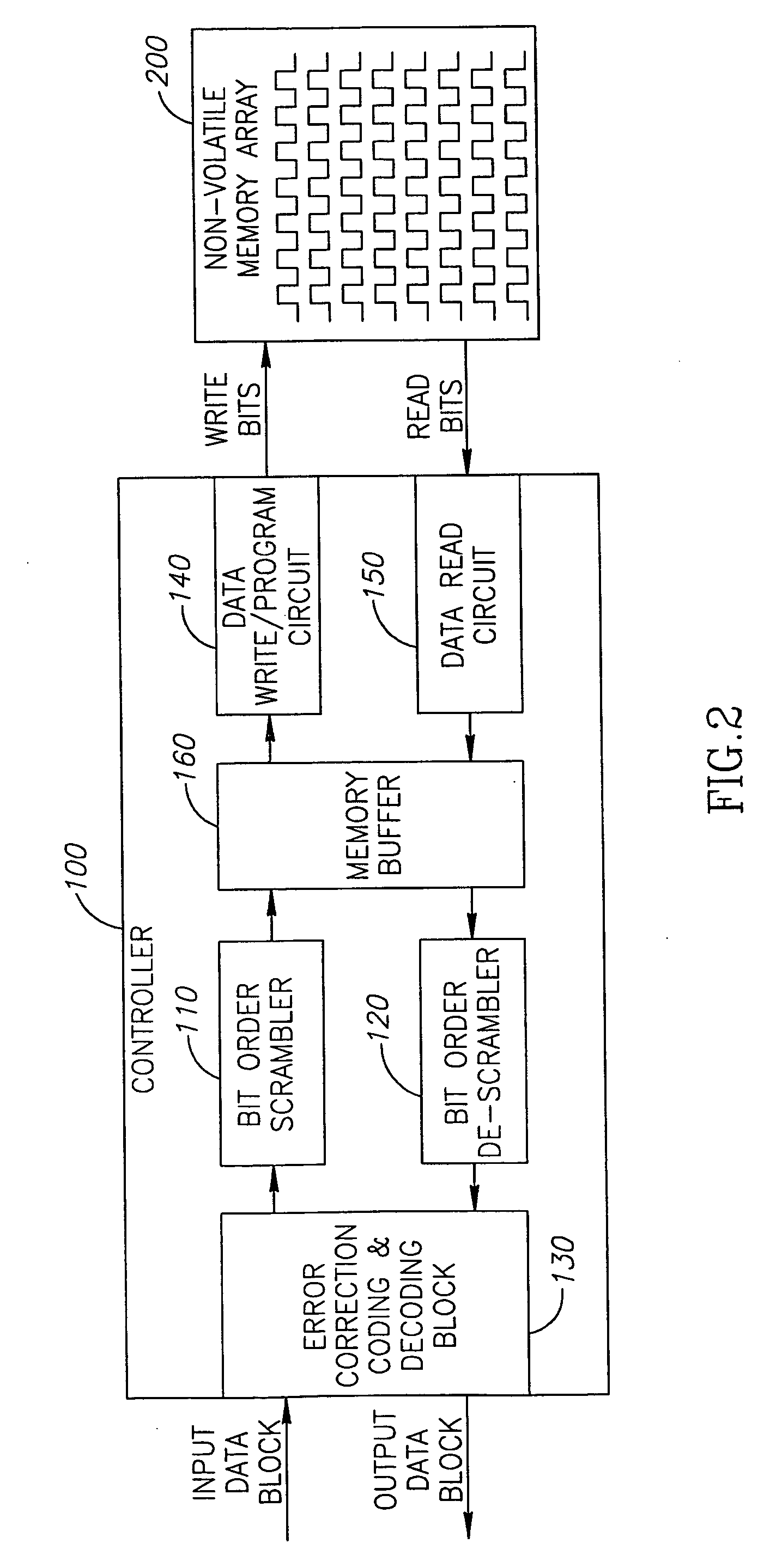
The present invention is a circuit, system, and method for rearranging data bits of a data block to be stored on an NVM array. The bits can be rearranged before or during an ECC is generated, or after an ECC is generated based on the original bits. The bits can be stored on the NVM array in their original order or in a rearranged order. When reading the bits from the NVM array, they can be rearranged in an inverse manner to the original arrangement to retrieve the original data bits. The original bits can be used to perform an ECC check and a correction function for the read bits. The technical effect of the invention is to improve the reliability and accuracy of data storage on NVM arrays.

Problems solved by technology

The problem with parity is that it discovers errors but does nothing to correct them.
Storage of multiple adjacent bits from a data stream or data block on a single NVM cell may have drawbacks relating to data recovery in the event the cell fails.

Method used


Image

  • Circuit, system and method for encoding data to be stored on a non-volatile memory array
  • Circuit, system and method for encoding data to be stored on a non-volatile memory array
  • Circuit, system and method for encoding data to be stored on a non-volatile memory array

Examples


Embodiment Construction

[0021]The present invention is a circuit, system and method for rearranging data bits of a data block to be stored on an NVM array. As part of some embodiments of the present invention, the bits may be rearranged (i.e. scrambled) according to a spreading pattern either before or during an ECC is generated, while in other embodiments of the present invention, bits may be rearranged after an ECC is generated based on the original bits. According to certain embodiments of the present invention, bits may be stored on the NVM array in the rearranged order, while in other embodiments of the present invention, bits may be stored on the NVM in their original order.

[0022]According to embodiments of the present invention, where bits are stored on an NVM array in a rearranged order, when reading bits from the NVM array, the read bits may be once again rearranged, in an inverse manner to that by which the data bits were rearranged before storing (i.e. unscrambled), in order to retrieve the orig...


PUM

PropertyMeasurementUnit
threshold voltagesaaaaaaaaaa
threshold voltageaaaaaaaaaa
dimensionsaaaaaaaaaa

Abstract

The present invention is a method, circuit and system for storing bits on a Non-Volatile Memory (“NVM”) array. According to some embodiments of the present invention, a bit scrambling block may rearrange the received block of bits according to a spreading pattern. An error correction code block may generate an error correction code (“ECC”) based on either the original block of bits or based on the rearranged block of bits, and a data storing circuit may store in the NVM array the ECC and the block of bits from which the ECC was not derived.

Description

FIELD OF THE INVENTION[0001]The present invention relates generally to non-volatile memory (“NVM”) devices. More particularly, the present invention relates to encoding or rearranging bits to be written to an NVM array.BACKGROUND OF THE INVENTION[0002]Non-Volatile Memory (“NVM”) cells come in a variety of cell structure, including “Floating Gate” and “Nitride Read Only Memory” (“NROM”). NVM cells generally are formed of transistors with programmable threshold voltages. The transistors have a threshold voltage (“Vt”) that is programmed or erased by charging or discharging a charge storage region located between a control gate and a channel in the transistor. Data is written in such memory cells by charging or discharging the charge storage region of the memory cell, so as to achieve threshold voltages corresponding to the data. An NVM cell may either be adapted to store a single bit in a single charge storage region, multiple bits in multiple charge storage regions, or multiple bits ...

Claims


Application Information

Patent Timeline
Patent Type & Authority Patents(United States)
IPC IPC(8): G06F12/02G06F12/16G11B
CPCG06F11/1008G06F2211/109
Inventor RAZ, MEIRAVCOHEN, ZEEVMARCU, ALON
Owner SAMSUNG ELECTRONICS CO LTD
Learn More