Semiconductor devices with reduced impact from alien particles

Inactive Publication Date: 2007-04-03
TAIWAN SEMICON MFG CO LTD
View PDF11 Cites 1 Cited by
  • Summary
  • Abstract
  • Description
  • Claims
  • Application Information

AI Technical Summary

Benefits of technology

[0007]In view of the foregoing, this disclosure provides an improved design of semiconductor devices. In one embodiment, an improved semiconductor device is disclosed with a NMOS transistor formed on a P-Well, in a deep N-well, a PMOS transistor formed on a N-Well, in the deep N-well,

Problems solved by technology

Semiconductor devices are unavoidably impacted by alien energy particles existing in the universe.
However, as cell geometries shrink, one problem arises.
The charge, which is stored as data, is now so small that its data integrity is now extremely susceptible to disturbance from electrical noise o

Method used


Image

  • Semiconductor devices with reduced impact from alien particles
  • Semiconductor devices with reduced impact from alien particles
  • Semiconductor devices with reduced impact from alien particles

Examples


Example

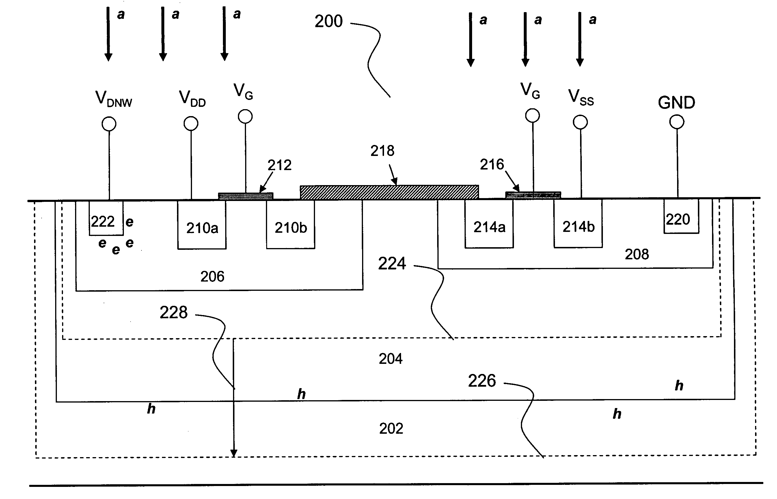
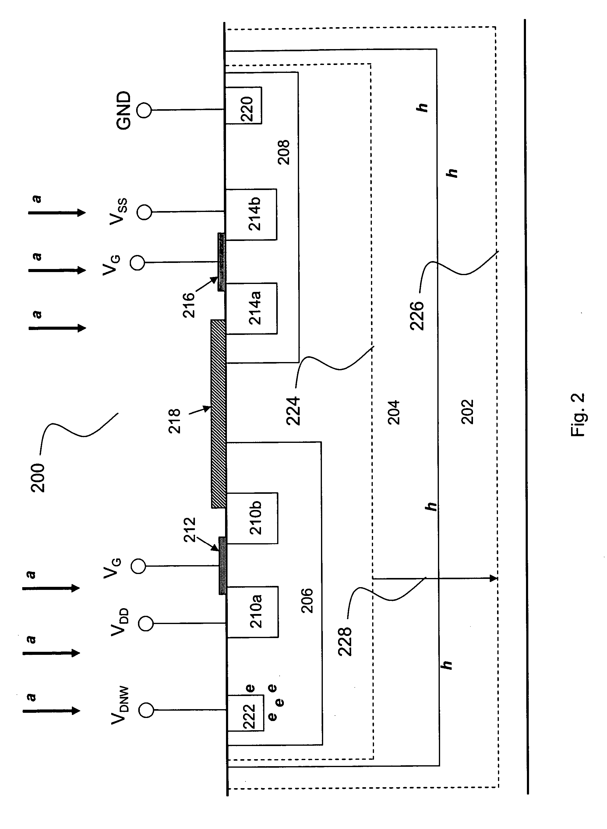
[0012]This disclosure provides an improved design of semiconductor devices with reduced impact from alien energized particles. The following illustration uses a memory device as an example to show how such an improved device will reduce soft error rate in a memory device. However, it is understood that the principle of this invention applies to any small size devices.

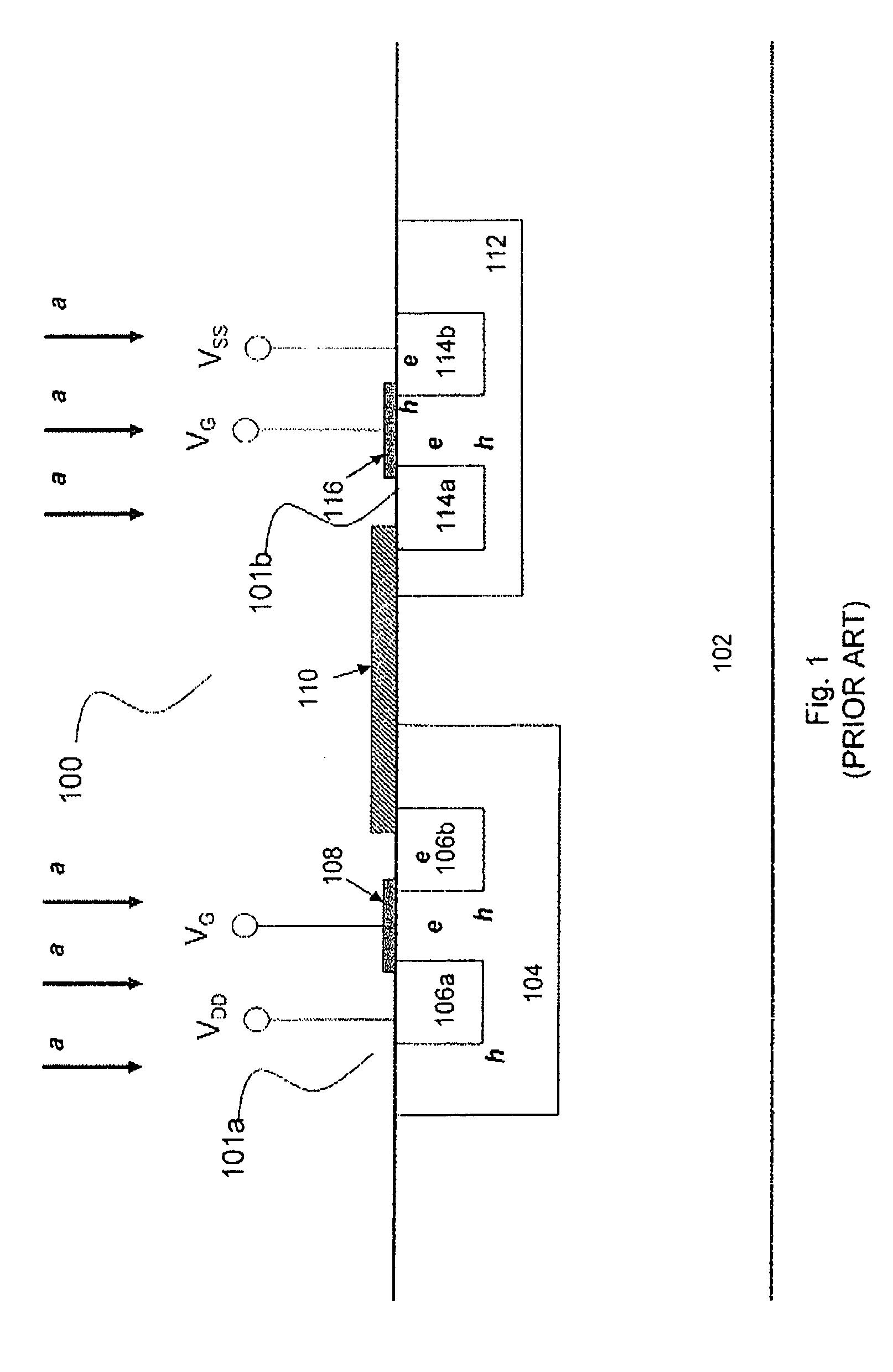
[0013]FIG. 1 illustrates a portion of a cross-sectional view of the physical construction of a conventional semiconductor memory circuit 100. Shown in this figure is a p-channel metal oxide semiconductor (PMOS) transistor 101a connected to a n-channel metal oxide semiconductor (NMOS) transistor 101b. The two transistors are built and located upon a lightly p-doped silicon substrate 102. The PMOS transistor is built within a n-doped well region (N-well) 104 typically created by the ion implantation of a n-type doping material. The p-doped, P+ source 106a and P+ drain 106b regions of the PMOS transistor are shown located ...


PUM


Abstract

An improved semiconductor device is disclosed with a NMOS transistor formed on a P-Well in a deep N-well, a PMOS transistor formed on a N-Well in the deep N-well, a first voltage coupled to a source node of the PMOS, and a second voltage higher than the first voltage coupled to the N-well, wherein the second voltage expands a depletion region associated with the PMOS and NMOS transistor for absorbing electrons and holes caused by alien particles.

Description

BACKGROUND [0001]The present disclosure relates generally to semiconductor devices and more particularly, to the improved semiconductor devices with reduced impact from alien particles.[0002]Semiconductor devices are unavoidably impacted by alien energy particles existing in the universe. For example, the cosmic ray contains high-energy neutrons, which may strike some isotopes in the device package and semiconductor device to release alpha particles. These energized particles will impact the performance of semiconductor devices.[0003]For example, taking semiconductor memories, they are comprised of large arrays of individual memory cells. Each memory cell stores a “0” or a “1” data bit as an electrical low or high voltage state. At least 8 data bits may compose a data byte. At least 16 data bits may compose a data word. In each memory operation cycle, at least one byte is typically written into, or read from the memory array. Cells are physically arranged as vertical data (bit lines...

Claims


Application Information

Patent Timeline
IPC IPC(8): H01L29/76
CPCG11C11/4125H01L27/0921H01L27/11H01L27/1104H01L2924/0002H01L2924/00H10B10/00H10B10/12
Inventor LEE, CHUNG-JUNGONG, TONG-CHERN
Owner TAIWAN SEMICON MFG CO LTD
Why Eureka
Try Eureka