
Photoelectric conversion device

A photoelectric conversion element and electrode technology, which is applied in the direction of electrical components, photovoltaic power generation, and electric solid-state devices, can solve problems such as high practicability, safety issues, and inability to obtain performance, and achieve high practicability, improved design, and freedom. The effect of increasing

Inactive Publication Date: 2007-12-12
DAI ICHI KOGYO SEIYAKU CO LTD
View PDF2 Cites 4 Cited by
  • Summary
  • Abstract
  • Description
  • Claims
  • Application Information

AI Technical Summary

Problems solved by technology

(SeCN) 2 / SeCN - Compared with it, although it shows higher performance, it has problems in terms of safety, and it cannot be said that it is very practical.
[0010] In addition, among redox pairs that can be used in photoelectric conversion elements other than iodine, Br 2 / Br - , Fe(CN) 6 4- / Fe(CN) 6 3- , Fe 2+ / Fe 3+ , S 2- / S n 2- 、Se 2- / Se n 2- , V 2+ / V 3+ , quinone / hydroquinone, etc. However, there are problems in performance, stability, safety, etc., and the performance comparable to iodine cannot be obtained

Method used


Image

  • Photoelectric conversion device
  • Photoelectric conversion device
  • Photoelectric conversion device

Examples


Embodiment 1

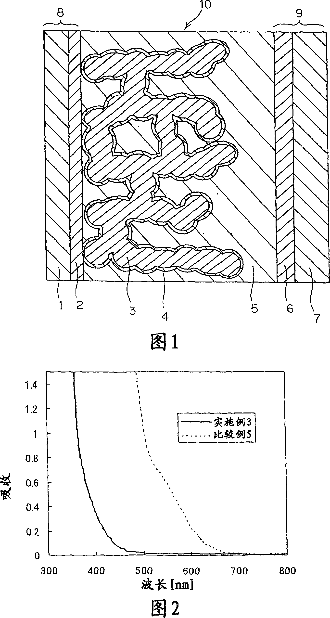
[0137] [Production of Porous Metal Oxide Semiconductor]

[0138] SnO doped with fluorine was formed by vacuum evaporation on a transparent substrate 1 made of glass. 2 To form the transparent conductive film, the porous metal oxide semiconductor layer 3 was formed on the transparent conductive film 2 by the following method.

[0139]As the electrode substrate 8 on which the transparent conductive film 2 is formed on the transparent substrate 1, FTO glass (manufactured by Nippon Sheet Glass Co., Ltd.) is used, and the film thickness of about 6 μm and the area of ​​about 5 mm×10 mm are formed on the surface by the screen printing method. On the surface of the transparent conductive film 2 side, print a commercially available titanium oxide paste (manufactured by Catalyst Chemicals Co., Ltd., trade name: TSP-18NR, particle size 20nm), and then use the screen printing method on the same area, A commercially available titanium oxide paste (manufactured by Catalyst Kasei Co., Ltd.,...

Embodiment 2

[0149] A solar cell was produced in the same manner as in Example 1 except that 1-methyl-3-ethylimidazolium bis(trifluoromethanesulfonyl)imide was used as the solvent for the electrolyte layer 5 .

Synthetic example

[0171] A synthesis example of the redox couple of the present invention will be given below, but the synthesis method is not limited thereto, and known materials and synthesis methods can be used for production.

[0172] [Redox Pairs: Synthesis of Reductants]

[0173] Dissolve 1 molar equivalent of 5-methyl-2-mercapto-1,3,4-thiadiazole and 0.5 molar equivalent of potassium carbonate in methanol, and perform ultrasonic bath treatment while stirring until the potassium carbonate dissolves and disappears until (about 2.5 hours). Thereafter, the solid was removed using filter paper, the solvent was distilled off with a rotary evaporator, and the resulting white solid was washed with dichloromethane, followed by vacuum drying to synthesize 5-methyl-2-mercapto-1. 3,4-thiadiazole potassium salt. The reaction yield was 70%.

[0174]Next, 1 molar equivalent of the synthesized compound (concentration: 1M) was dissolved in acetone, and a solution (concentration: 1M) of 1 molar equival...


PUM

PropertyMeasurementUnit
Film thicknessaaaaaaaaaa

Abstract

A photoelectric transformation device is provided to obtain photoelectric transformation efficiency and stability equal to a device utilizing a conventional iodine-based oxidation-reduction pair by using an oxidation-reduction pair in a photoelectric transformation device like a dye-sensitized solar cell. A photoelectric transformation device(10) includes a semiconductor electrode, a counter electrode(9) and an electrolyte layer(5) between the semiconductor electrode and the counter electrode. The electrolyte layer is an oxidation-reduction pair and includes a compound indicated by the following reaction formula 1. A-S^ M^+ A-S-S-A (reaction formula 1). In the reaction formula1, M^+ is an organic or inorganic positive ion and A is an aromatic, non-aromatic, complex aromatic or a complex non-aromatic annular compound. The counter electrode contains a conductive polymer catalyst having catalyst activity with respect to the oxidation-reduction pair.

Description

technical field [0001] The present invention relates to a photoelectric conversion element suitable for use as a dye-sensitized solar cell or the like. Background technique [0002] In recent years, various solar cells have been proposed as photoelectric conversion elements that convert light energy into electrical energy. Among them, the dye-sensitized solar cell published by Graetzel et al. of Lausanne University in Switzerland in "Nature" 1991, 353, p737-740, etc. in 1991 is expected to be practical as a low-cost solar cell because the materials and processes used are cheap. change. [0003] Dye-sensitized solar cells are generally composed of: a semiconductor electrode having a photoelectric conversion layer composed of a semiconductor adsorbed with dye on a conductive substrate; The counter electrode of the catalyst layer and the electrolyte layer held between these semiconductor electrodes and the counter electrode are constituted. [0004] As an electrolyte for dye...

Claims


Application Information

Patent Timeline
IPC IPC(8): H01L51/42H01L51/46H01G9/20H01G9/022H01M14/00
CPCY02E10/542Y02E10/549H01G9/2018
Inventor 齐藤恭辉菊田学河野通之
Owner DAI ICHI KOGYO SEIYAKU CO LTD
Learn More