Semiconductor package with heat dissipating structure and method of manufacturing the same

a technology of heat dissipation structure and semiconductor, which is applied in the direction of semiconductor/solid-state device details, horticulture tools/apparatus, semiconductor devices, etc., can solve the problem of inefficient heat dissipation with the conventional bga package structure, and achieve the effect of improving the reliability of the operation of electronic components

Active Publication Date: 2007-04-10
SAMSUNG ELECTRONICS CO LTD
View PDF15 Cites 18 Cited by
  • Summary
  • Abstract
  • Description
  • Claims
  • Application Information

AI Technical Summary

Benefits of technology

[0016]The invention provides a semiconductor package with a heat dissipating structure in which heat generated by the operation of electronic components formed in a semiconductor chip is efficiently dissipated by providing various heat dissipating means; the reliability of the operation of the electronic components can be improved; and the semiconductor chip can be prevented from being pressed by a mold when the semiconductor package is encapsulated by encapsulant resin after arranging the heat dissipating means. The invention also provides a method of manufacturing the semiconductor package.

Problems solved by technology

Accordingly, thermal dissipation is not efficient with the conventional BGA package structure.

Method used


Image

  • Semiconductor package with heat dissipating structure and method of manufacturing the same
  • Semiconductor package with heat dissipating structure and method of manufacturing the same
  • Semiconductor package with heat dissipating structure and method of manufacturing the same

Examples


Embodiment Construction

[0024]The present invention will now be described more fully hereinafter with reference to the accompanying drawings, in which preferred embodiments of the invention are shown. This invention may, however, be embodied in many different forms and should not be construed as limited to the embodiments set forth herein. Rather, these embodiments are provided so that this disclosure will be thorough and complete, and will fully convey the scope of the invention to those skilled in the art. Like numbers refer to like elements throughout the specification.

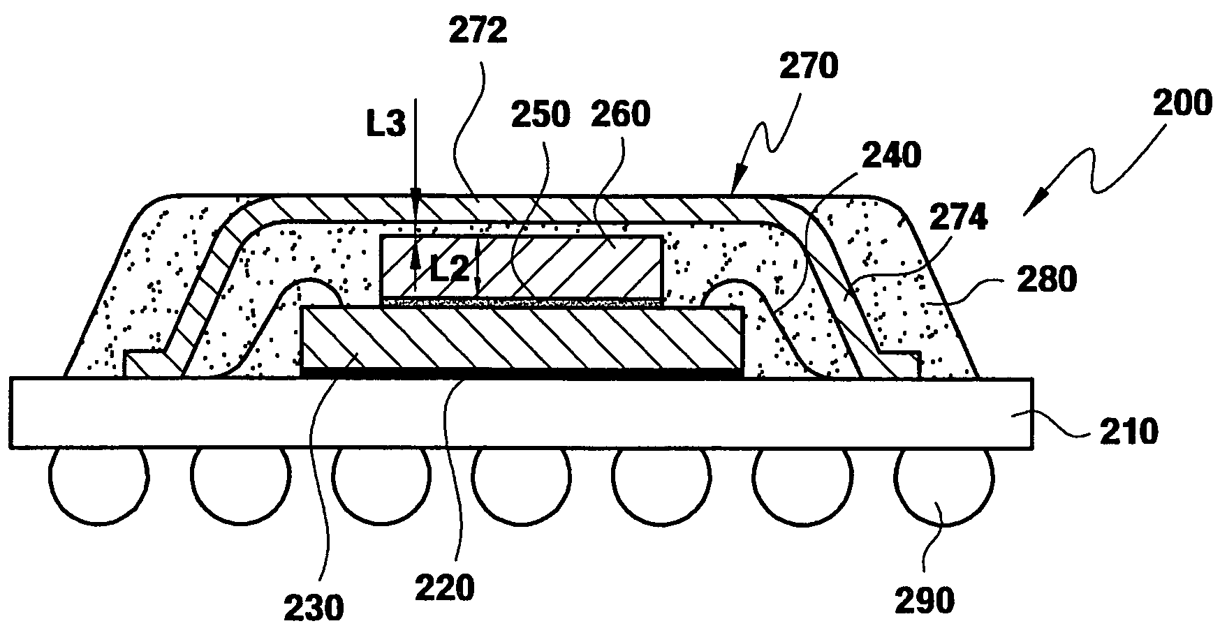
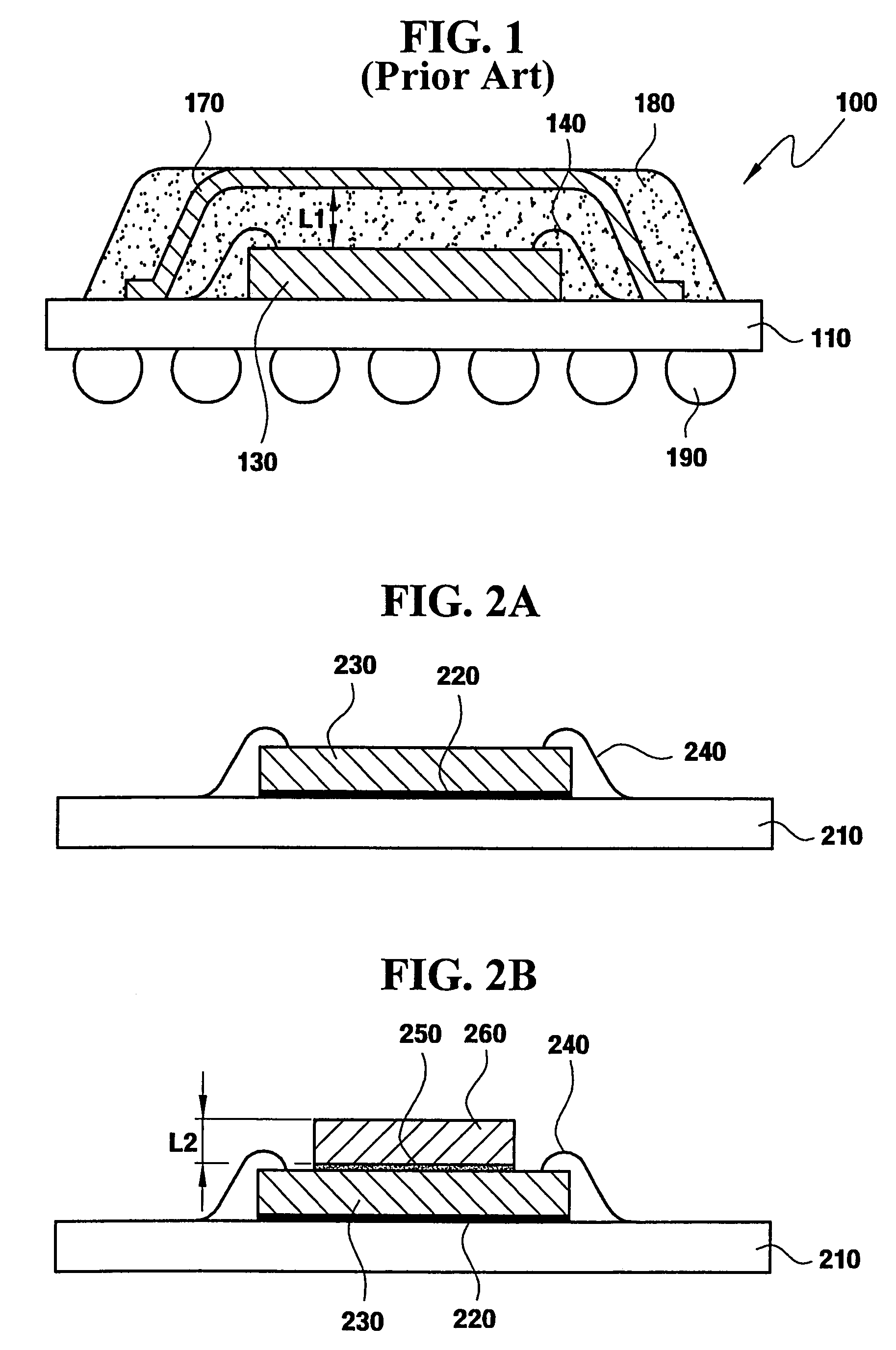
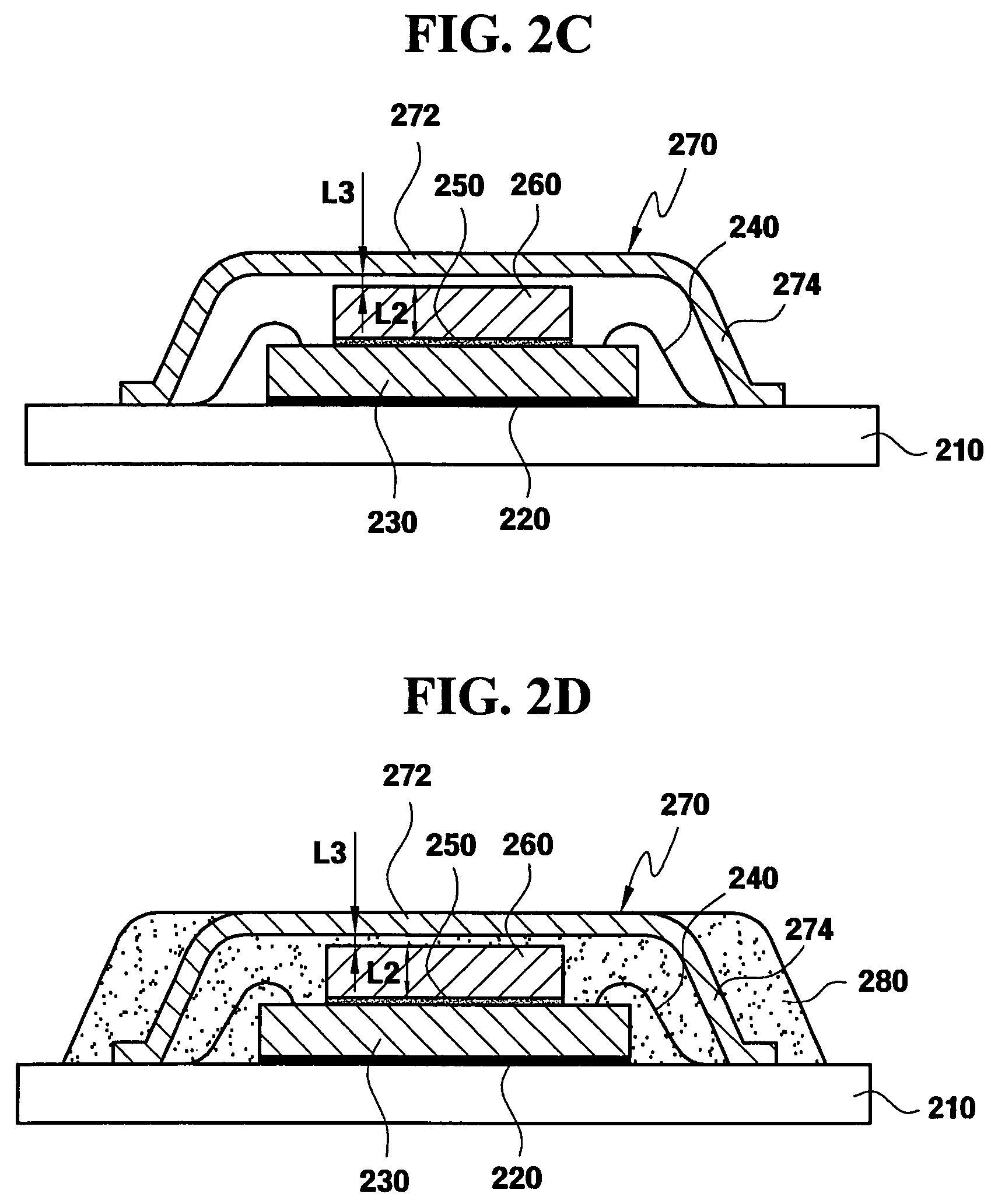
[0025]Semiconductor packages according to embodiments of the present invention constitute high-frequency microprocessors or ASIC products, or high-speed semiconductor memory devices such as DRAMs or SRAMs. Such devices mostly have input / output terminals with multiple pins. Semiconductor packages constituting such devices can be classified according to the multiple pin configurations, for example, a plastic or ceramic pin grid array (PGA) ...


PUM


Abstract

A semiconductor package in which heat is easily dissipated and a semiconductor chip is not damaged during a molding process, and a method of manufacturing the same. The semiconductor package with a heat dissipating structure includes a substrate, a semiconductor chip, which is mounted on the substrate and electrically connected with the substrate by bonding means, a heat slug which is adhered to the semiconductor chip and formed of a thermally conductive material, and a heat spreader partially exposed to the outside of the semiconductor package, and which is formed on the heat slug to be spaced a buffer gap apart from the heat slug.

Description

[0001]This application claims priority of Korean Patent Application No. 10-2004-0005464 filed on Jan. 28, 2004 in the Korean Intellectual Property Office, the disclosure of which is incorporated herein in its entirety by reference.BACKGROUND OF THE INVENTION[0002]1. Field of the Invention[0003]The present invention relates to a semiconductor package with a heat dissipating structure and a method of manufacturing the same, and more particularly, to a semiconductor package with a heat dissipating structure and a method of manufacturing the same for preventing malfunction of a semiconductor chip due to a hindrance in thermal dissipation when needing to rapidly dissipate heat that is generated during a high-speed operation of the semiconductor chip to the outside of the package using a heat spreader and a heat slug.[0004]2. Description of the Related Art[0005]Generally, thermal dissipation is an important characteristic of semiconductor packages used by high-speed, high-frequency applic...

Claims


Application Information

Patent Timeline
Patent Type & Authority Patents(United States)
IPC IPC(8): H01L23/34H01L23/28H01L23/31H01L23/36H01L23/433
CPCH01L23/3128H01L23/4334H01L2224/48227H01L2224/73265H01L2924/01079H01L2924/1433H01L2924/15311H01L2924/16152H01L24/48H01L2924/14H01L2924/181H01L2224/45124H01L2224/45147H01L2924/00014H01L2224/45144H01L24/45H01L2924/00H01L2924/00012H01L2224/45015H01L2924/207A01G9/12A01G17/06A01G17/10A01G7/06
Inventor SEO, JEONG-WOO
Owner SAMSUNG ELECTRONICS CO LTD
Why Eureka
Try Eureka