

Method of manufacturing a semiconductor device comprising stacked chips and a corresponding semiconductor device
a manufacturing method and semiconductor technology, applied in semiconductor devices, semiconductor/solid-state device details, electrical apparatus, etc., can solve the problems of inability to further reduce the external dimensions the cost of the semiconductor memory device, and achieve the effect of reducing the stack heigh
- Summary
- Abstract
- Description
- Claims
- Application Information
AI Technical Summary
Benefits of technology
Problems solved by technology
Method used
Image

Examples
Embodiment Construction
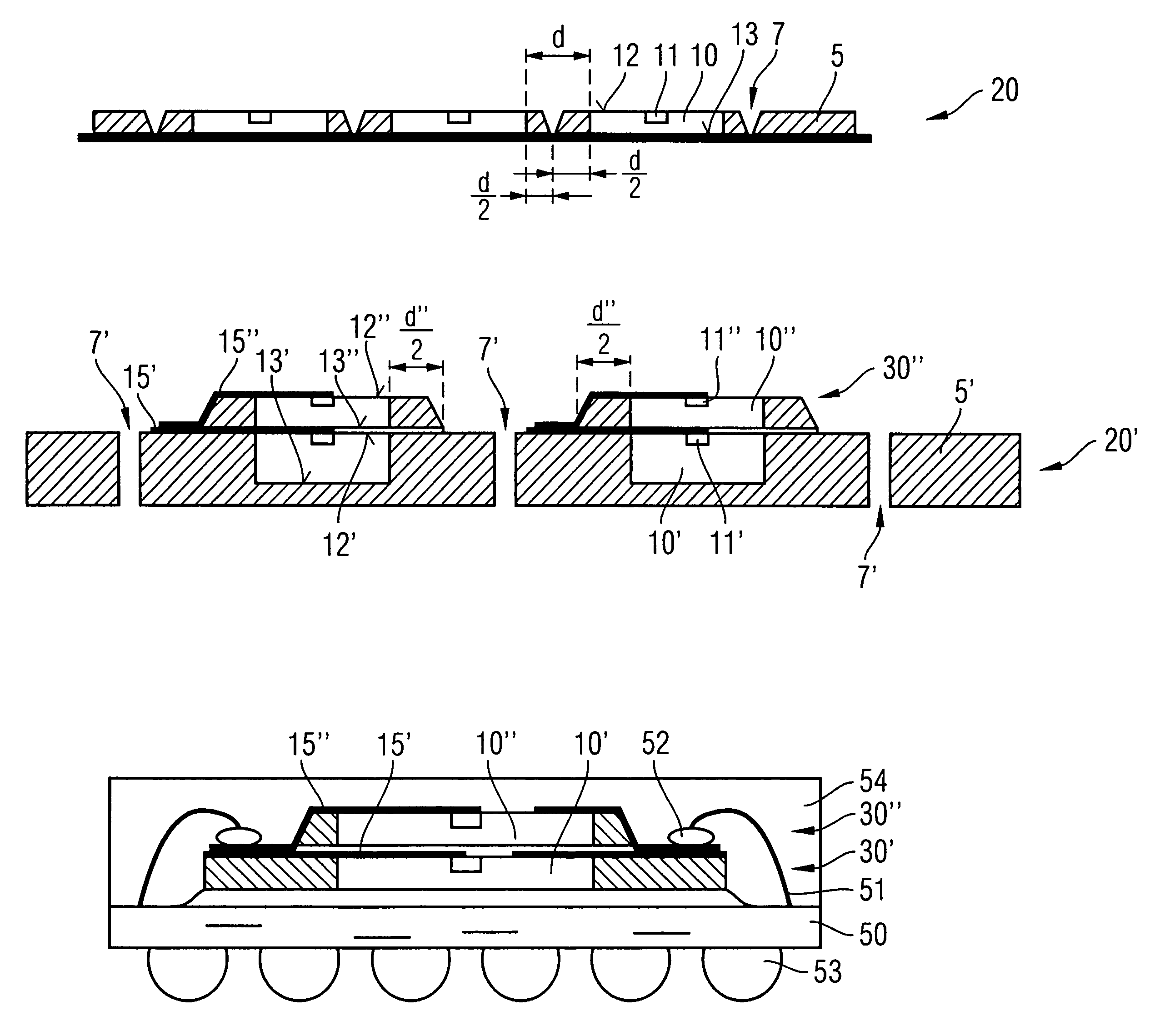
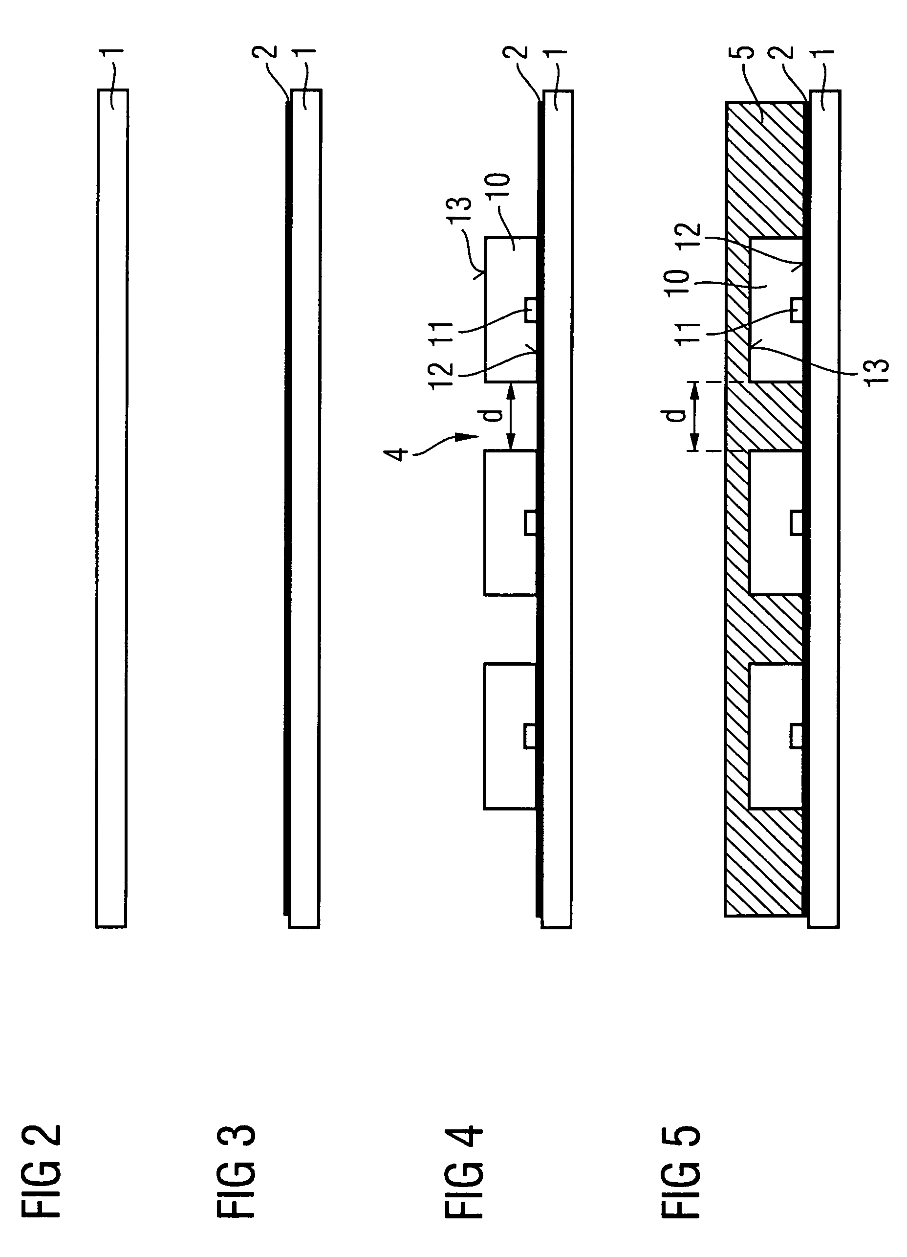
[0023]An intermediate carrier1 or a carrier plate is provided in a first step (FIG. 2). An adhesive layer 2 or an adhesive tape is attached to the intermediate carrier 1 (FIG. 3). One or more processed semiconductor wafers are diced and the individualized chips 10 are provided. These chips 10 may be identical in functionality and / or its dimensions or be different. The chips 10 are arranged on the intermediate carrier 1 horizontally spaced by a gap 4 between two neighboring chips 10. A width d of the gap 4 (distance between to neighboring chips 10) is preferably identical for all gaps 4 between neighboring chips 10. Each chip 10 is placed with its active surface 12 on the intermediate carrier 1. The active surface 12 is defined by the surface of the chip 10 which comprises contact pads 11. Thus, the active surface 12 is covered by the intermediate carrier 1 and a backside 13 opposite to the active surface 12 remains exhibited (FIG. 4).
[0024]In a subsequent step, a mould 5 is applied ...
PUM
 Abstract
Description
Claims
Application Information