Semiconductor light-emitting element and manufacturing method thereof

a technology of semiconductors and light-emitting elements, applied in the direction of semiconductor devices, basic electric elements, electrical appliances, etc., can solve the problems of large change step burden, achieve the effect of preventing surface roughening, preventing over-etching on the peripheral lower portion of the electrode, and improving the reliability of the electrod

Active Publication Date: 2007-05-01
DOWA ELECTRONICS MATERIALS CO LTD
View PDF7 Cites 6 Cited by
  • Summary
  • Abstract
  • Description
  • Claims
  • Application Information

AI Technical Summary

Benefits of technology

[0013]In view of the aforementioned circumstances, an object of the present invention is to provide a semiconductor light-emitting element capable of realizing an improvement in electrode reliability by preventing over-etching on a peripheral lower portion of an electrode by a chemical treatment while maintaining the flow of steps in which a surface roughening treatment by the chemical treatment is performed after the electrode is formed on a semiconductor substrate, and a manufacturing method thereof.
[0019]According to a semiconductor light-emitting element of the present invention, a non-roughened surface region which prevents surface roughening by a surface roughening treatment including a chemical treatment is secured in a peripheral portion of an electrode. Therefore, over-etching on a peripheral lower portion of the electrode can be prevented, thereby improving the reliability of the electrode. Moreover, since the non-roughened surface region is secured in the peripheral portion of the electrode, the surface roughening treatment including the chemical treatment can be performed after the electrode is formed on the semiconductor substrate. Therefore, it is unnecessary to greatly change the conventional flow of steps, and hence the burden of changing the steps is small.
[0020]A manufacturing method of a semiconductor light-emitting element of the present invention comprises, forming an electrode, followed by covering selectively a surface of the electrode with a protective film, thereafter roughening the surface from above the protective film, and then removing the protective film. Accordingly over-etching on a peripheral lower portion of the electrode due to the surface roughening treatment including the chemical treatment can be prevented, thus improving the reliability of the electrode. Moreover, since the surface roughening treatment including the chemical treatment is performed after the electrode is formed, it is unnecessary to greatly change the conventional flow of steps, and hence the burden of changing the steps is small.

Problems solved by technology

Therefore, a conventional order of steps in which the surface roughening treatment is performed after the electrode forming process needs to be greatly changed, which causes a problem that the burden of changing the steps is large.

Method used


Image

  • Semiconductor light-emitting element and manufacturing method thereof
  • Semiconductor light-emitting element and manufacturing method thereof
  • Semiconductor light-emitting element and manufacturing method thereof

Examples


Embodiment Construction

)

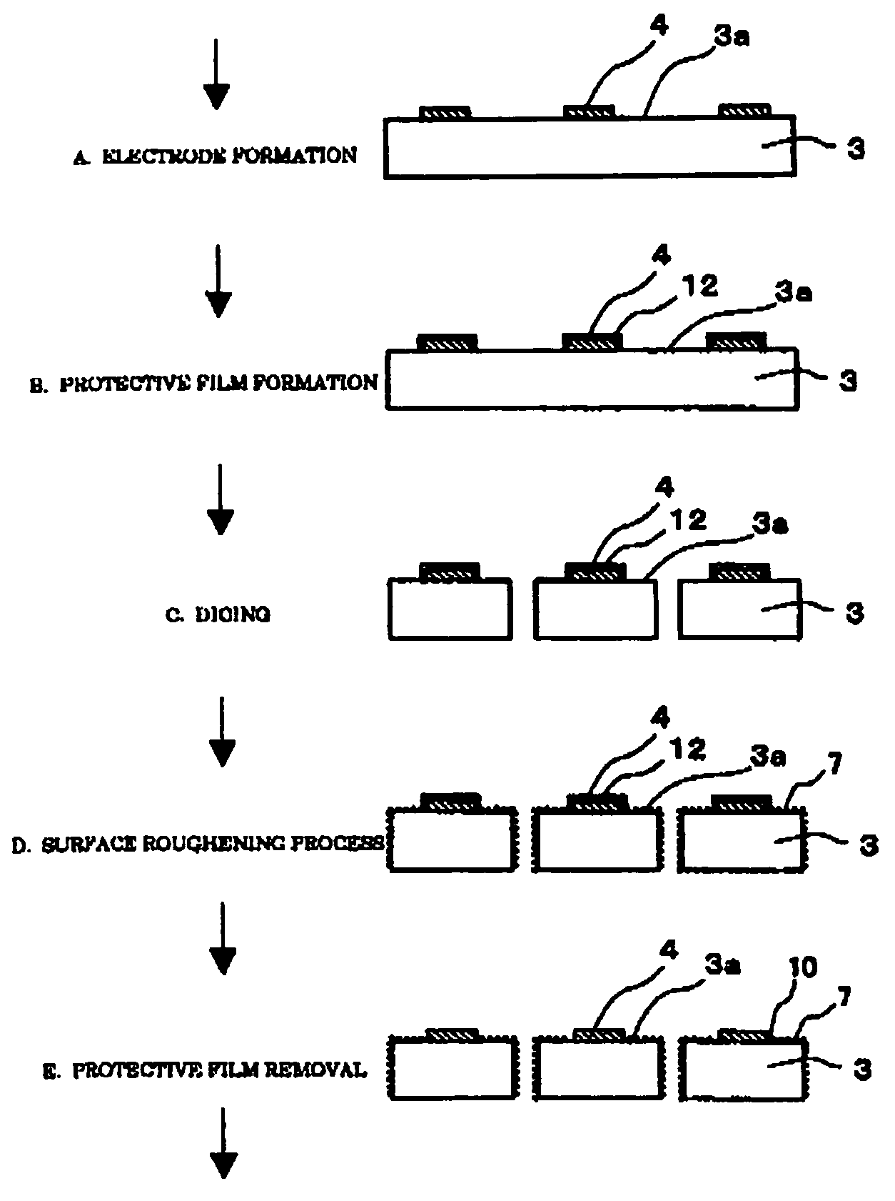
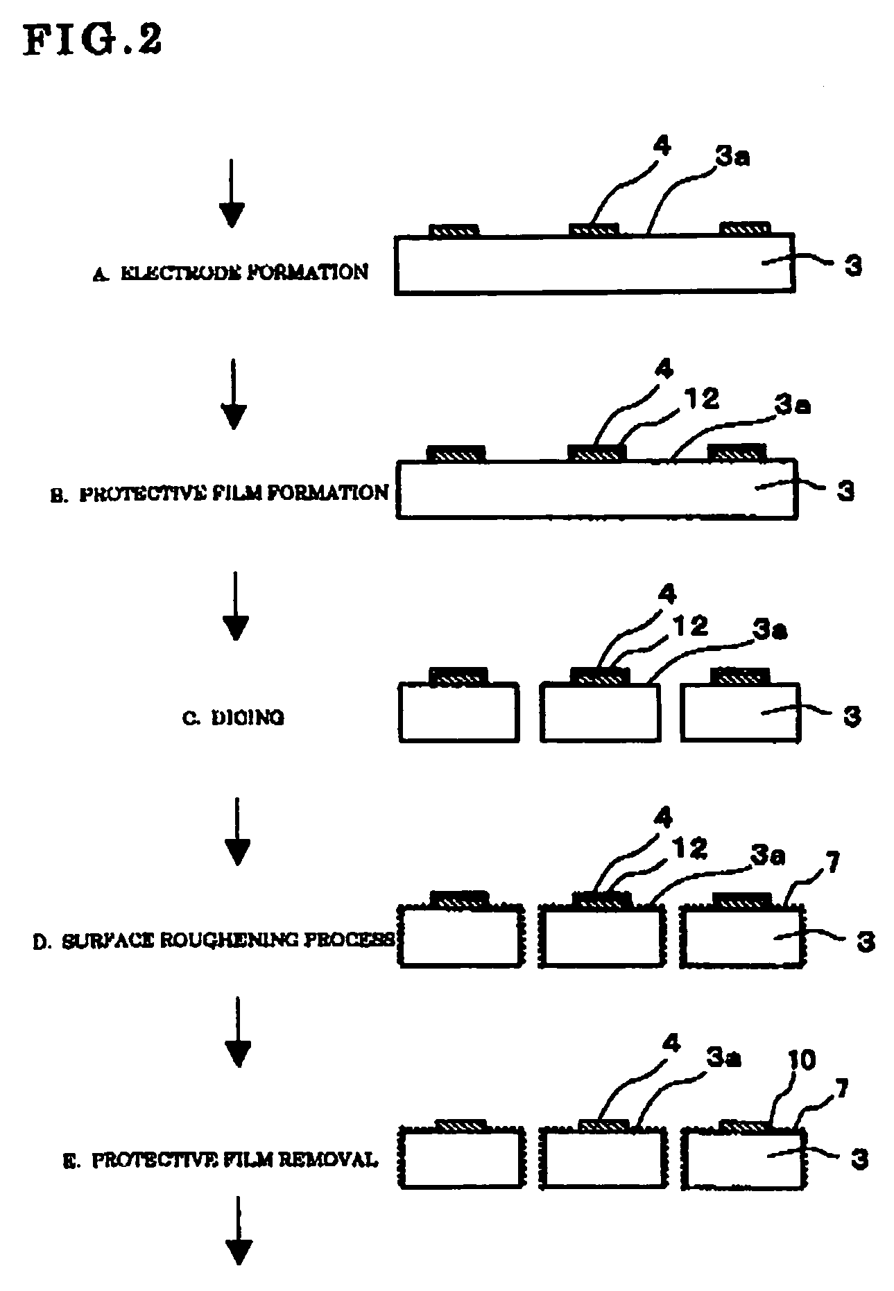
[0026]An embodiment of the present invention will be described below with reference to the drawings.

[0027]It should be mentioned that this embodiment will be explained with a case where a chemical treatment is used as a surface roughening treatment as an example.

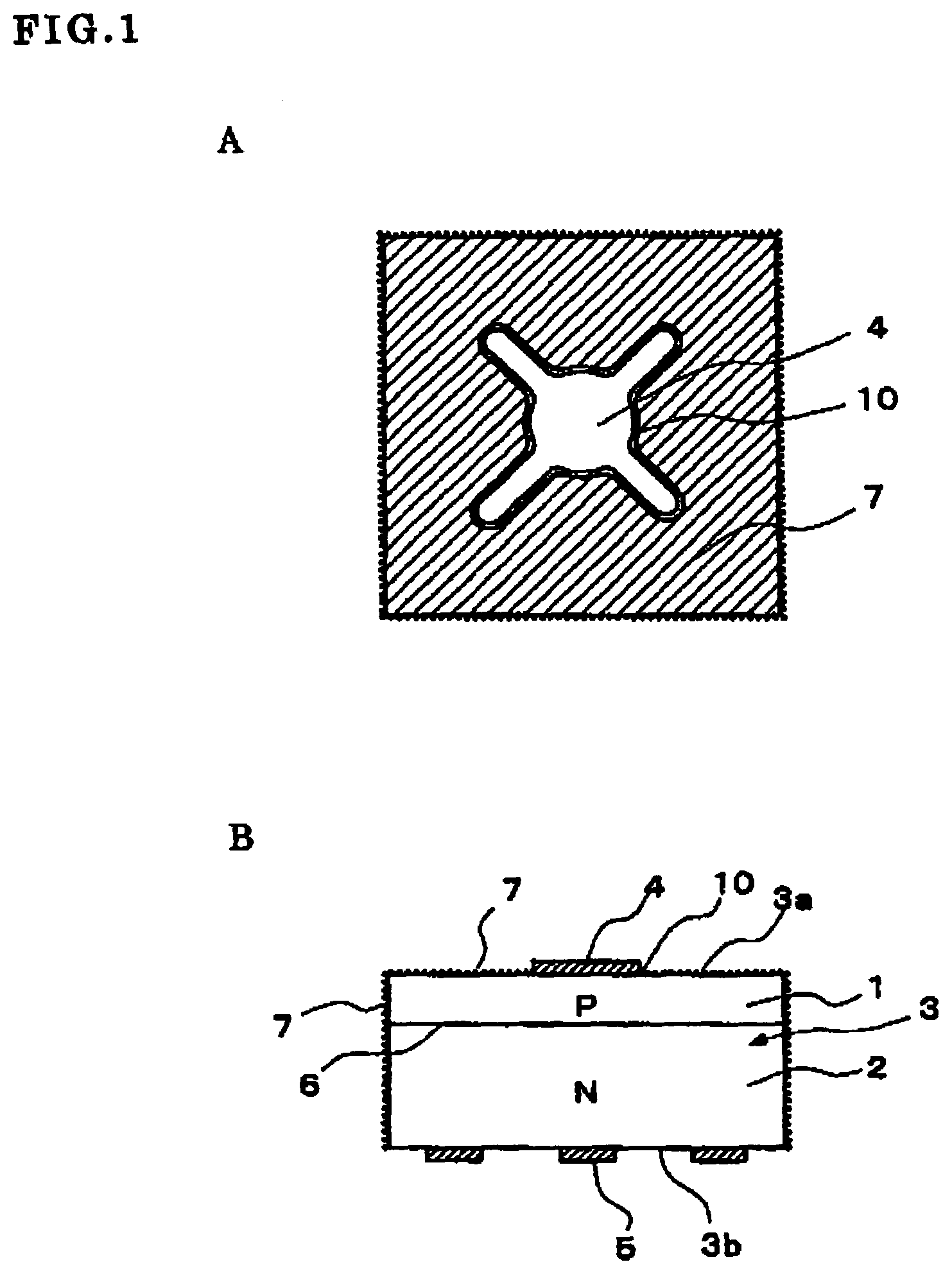
[0028]FIG. 1A is a plan view of a semiconductor light-emitting element according to the embodiment, FIG. 1B is a cross-sectional side view thereof, and FIG. 2A to FIG. 2E are views showing steps of a manufacturing method of the semiconductor light-emitting element according to the embodiment.

[0029]As shown in FIG. 1A and FIG. 1B, this semiconductor light-emitting element includes a semiconductor substrate (for example, AlGaAs) 3 having a PN junction 6 formed by a P-type semiconductor region (first semiconductor region) 1 and an N-type semiconductor region (second semiconductor region) 2, a P-side electrode 4, and at least one of N-side electrodes 5. The PN junction 6 at an interface between the P-type semiconductor region 1...


PUM


Abstract

An improvement in electrode reliability is realized by preventing over-etching on a peripheral lower portion of an electrode while maintaining the flow of steps of roughening a surface after forming the electrode on a semiconductor substrate. After a P-side electrode 4 is formed on a main surface 3a of a semiconductor substrate 3, a surface of the P-side electrode 4 is selectively covered with a protective film 12, after the semiconductor substrate 3 is cut into chips, the surface is roughened from above the protective film 12, the main surface 3a around the P-side electrode 4 and a side surface are roughened with a non-chemical treatment region 10 which is a non-roughened surface region being left in a peripheral portion of the P-side electrode 4 covered with the protective film 12, and thereafter the protective film 12 is removed.

Description

BACKGROUND OF THE INVENTION[0001]1. Field of the Invention[0002]The present invention relates to a semiconductor light-emitting element in which a roughened surface region which suppresses internal reflection of light is formed on a main ice of a semiconductor substrate from which light is taken out, and a manufacturing method thereof.[0003]2. Description of the Related Art[0004]The brightness is increased by forming a roughened surface which suppresses internal reflection of light on a main surface of a semiconductor light emitting element from which light is taken out (See Patent Document 1, for example).[0005]FIG. 3 shows an example thereof. This semiconductor light-emitting element (light-emitting diode) includes an AlGaAs semiconductor substrate 3, for example, composed of a P-type semiconductor region 1 and an N-type semiconductor region 2, a P-side electrode 4, and at least one of N-side electrodes 5. A PN junction 6 at an interface between the P-type semiconductor region 1 a...

Claims


Application Information

Patent Timeline
Patent Type & Authority Patents(United States)
IPC IPC(8): H01L29/22H01L33/22H01L33/30H01L33/36
CPCH01L33/22
Inventor SUNACHI, NAOYAMATSUOKA, HIROYUKI
Owner DOWA ELECTRONICS MATERIALS CO LTD
Why Eureka
Try Eureka