Non-volatile memory and fabricating method thereof

a technology of non-volatile memory and fabricating method, which is applied in the direction of basic electric elements, semiconductor devices, electrical equipment, etc., can solve the problems of increasing the size of each device as well as the other, and no solution, so as to reduce the width of source/drain region and overlying dielectric strip, the overall level of integration of the device can be increased, and the selectivity of different etchings can be reduced.

Active Publication Date: 2007-05-08
MACRONIX INT CO LTD
View PDF3 Cites 8 Cited by
  • Summary
  • Abstract
  • Description
  • Claims
  • Application Information

AI Technical Summary

Benefits of technology

[0006]Accordingly, at least one objective of the present invention is to provide a method of fabricating a non-volatile memory capable of resolving the misalignment problem in the conventional process of forming contacts.
[0007]At least a second objective of the present invention is to provide a non-volatile memory having a smaller device dimension so that overall level of integration of the memory can be increased.
[0009]In the present invention, sidewall spacers are formed inside the openings between neighboring dielectric strips. Furthermore, the spacers and the dielectric strips have different etching selectivity. Hence, the spacers on the sidewalls of the dielectric strips are able to provide a better protection in the process of forming the contact openings. In other words, the spacers permit the fabrication of self-aligned contacts. Therefore, the problem of having a misalignment between the contact and the source / drain region is resolved so that the contact can have a larger processing window.
[0011]Because a etching stopped layer is disposed between two neighboring dielectric strips and that the etching stopped layer and the dielectric strips have different etching selectivity, misalignment between the contact and the source / drain region is minimized in the process of forming the contact in the dielectric layer and the dielectric strips. Therefore, the width of the source / drain region and the overlying dielectric strip can be reduced and overall level of integration of the devices can be increased.

Problems solved by technology

However, because the source / drain regions are buried within the substrate, contacts are required to connect the source / drain regions electrically with an external circuit.
Although the misalignment problem can be ameliorated through an increase in the width of the source / drain regions, this also increases the size of each device as well.
Hence, from the point of view of device integration, this is no a solution.

Method used


Image

  • Non-volatile memory and fabricating method thereof
  • Non-volatile memory and fabricating method thereof
  • Non-volatile memory and fabricating method thereof

Examples


Embodiment Construction

[0021]Reference will now be made in detail to the present preferred embodiments of the invention, examples of which are illustrated in the accompanying drawings. Wherever possible, the same reference numbers are used in the drawings and the description to refer to the same or like parts.

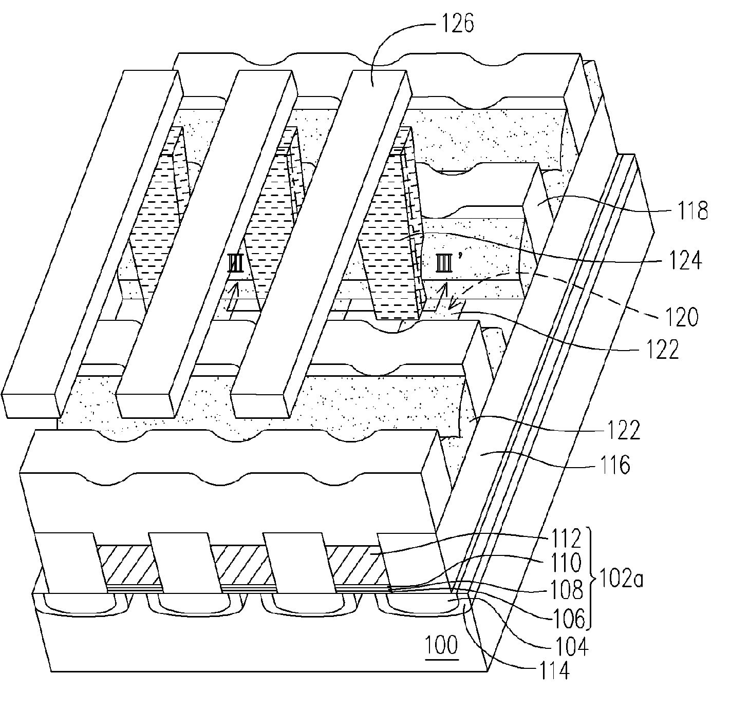
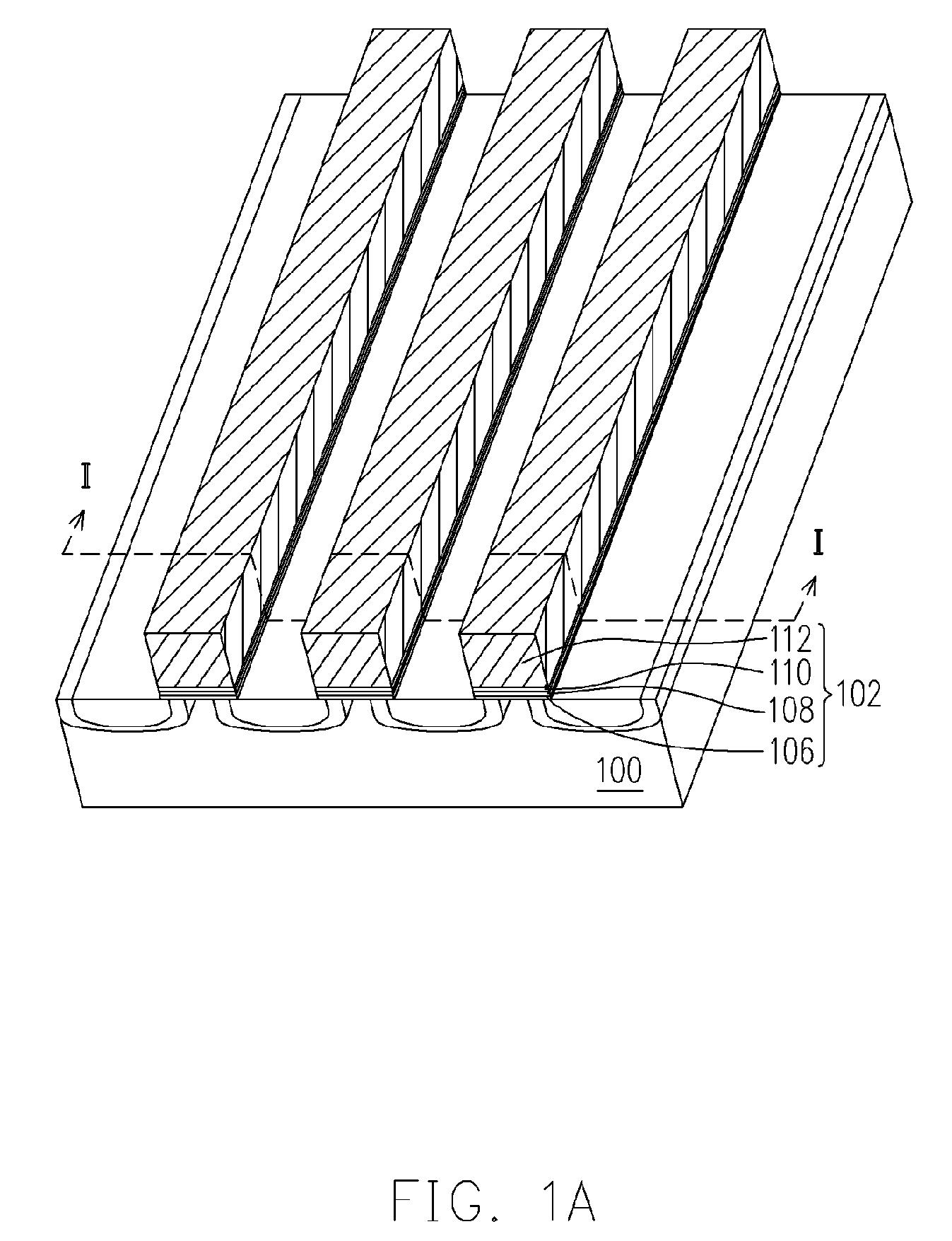
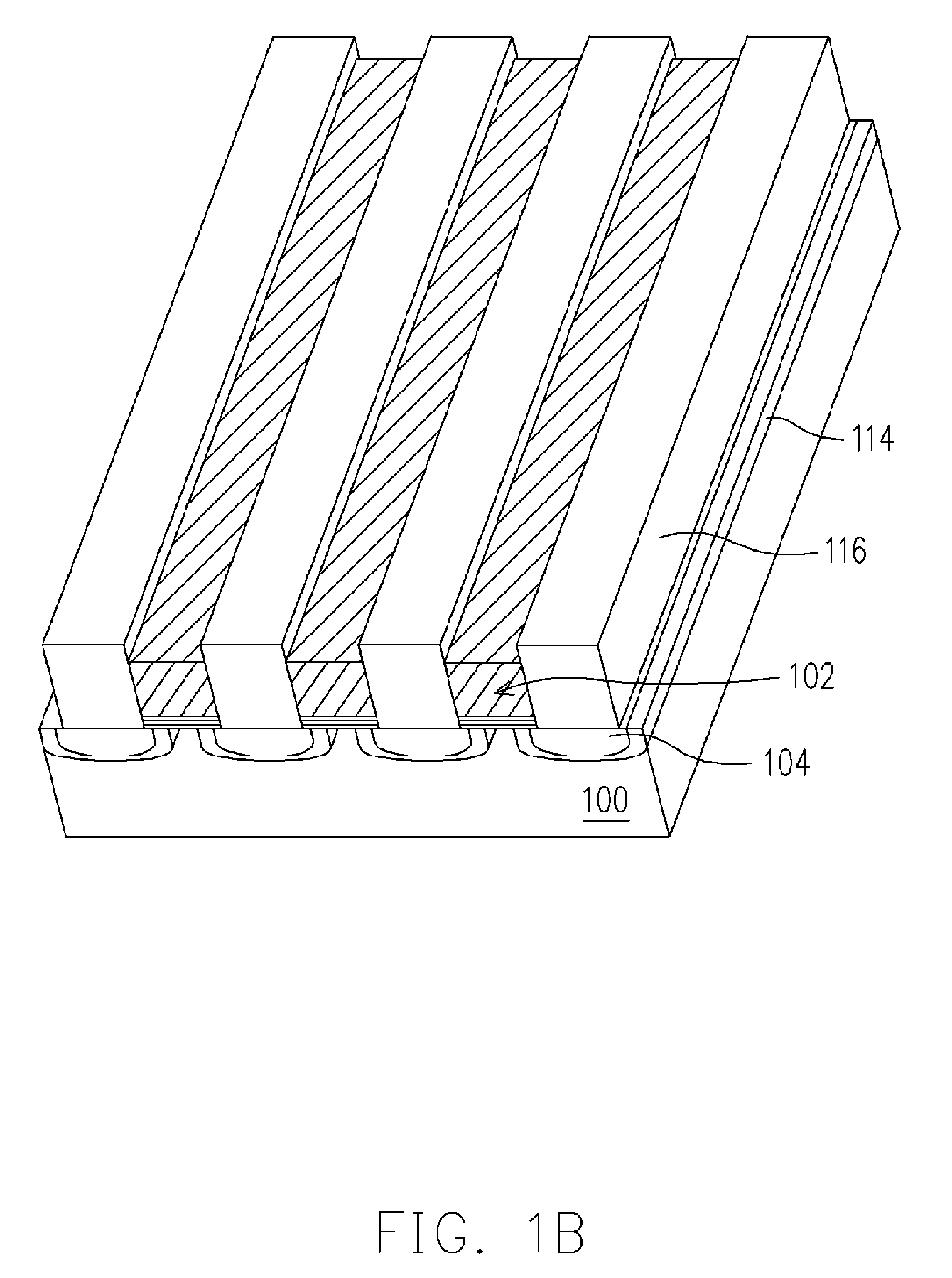
[0022]FIGS. 1A through 1E are perspective views showing the steps for fabricating a non-volatile memory according to one preferred embodiment of the present invention. As shown in FIG. 1A, a bottom dielectric layer 106, a charge storage layer 108, a top dielectric layer 110, a control gate layer 112 and a mask layer (not shown) are sequentially formed over a substrate 100. Thereafter, the film layers are patterned to form a plurality of stack gate strips 102 and a plurality of mask strip layers (not shown). Each stack gate strip 102 comprises a bottom dielectric layer 106, a charge storage layer 108, a top dielectric layer 110 and a control gate layer 112 sequentially stacked over the substrate 100. ...


PUM


Abstract

A method of fabricating a non-volatile memory is provided. A plurality of stack gate strips is formed on a substrate and a plurality of source / drain regions is formed in the substrate beside the stack gate strips. A plurality of dielectric strips is formed on the source / drain regions. A plurality of word lines is formed on the stack gate strips and the dielectric strips. Thereafter, the stack gate strips exposed by the word lines are removed to form a plurality of openings. A plurality of spacers is formed on the sidewalls of the openings and the word lines. A dielectric layer is formed over the substrate. A plurality of contacts is formed in the dielectric layer and the dielectric strips between two adjacent word lines.

Description

BACKGROUND OF THE INVENTION[0001]1. Field of the Invention[0002]The present invention relates to a memory device and fabricating method thereof. More particularly, the present invention relates to a non-volatile memory (ROM) and fabricating method thereof.[0003]2. Description of the Related Art[0004]Non-volatile memory is a type of memory that permits multiple data writing, reading and erasing operations. Moreover, the stored data will be retained even after power to the device is removed. With these advantages, non-volatile memory has become one of the most widely adopted memory devices for personal computer and electronic equipment. Furthermore, non-volatile memory also has the advantages of occupying a small volume, having a fast access speed and consuming very little power. In addition, data can be erased in a block-by-block fashion so that the operating speed is further enhanced.[0005]A typical non-volatile memory comprises an array of memory cells. The horizontally laid memory...

Claims


Application Information

Patent Timeline
Patent Type & Authority Patents(United States)
IPC IPC(8): H01L29/792
CPCH01L27/115H01L27/11521H01L27/11568H01L27/0207H10B69/00H10B41/30H10B43/30
Inventor HAN, TZUNG-TINGCHEN, MING-SHANGLU, WEN-PINWENG, MENG-HSUAN
Owner MACRONIX INT CO LTD
Why Eureka
Try Eureka