Non-volatile memory and fabricating method thereof

a non-volatile memory and fabrication method technology, applied in the direction of basic electric elements, semiconductor devices, electrical equipment, etc., can solve problems such as reducing device reliability, and achieve the effect of increasing the process window

Active Publication Date: 2007-01-11
MACRONIX INT CO LTD
View PDF7 Cites 1 Cited by
  • Summary
  • Abstract
  • Description
  • Claims
  • Application Information

AI Technical Summary

Benefits of technology

[0006] Accordingly, at least one objective of the present invention is to provide a method of fabricating a non-volatile memory capable of resolving the misalignment problem in the conventional contact fabricating process.
[0007] At least a second objective of the present invention is to provide a non-volatile memory having a smaller device dimension so that overall level of integration of the memory can be increased.
[0010] Because contacts (the first conductive layers) are formed in the first dielectric layers on the isolation structures, misalignment between contacts and the source region or the drain region is minimized in the process of forming contacts, and the process window can be increased.

Problems solved by technology

However, in the process of forming such contacts, misalignment between the contacts and the source regions or the drain regions occurs easily, which would reduce device reliability.

Method used


Image

  • Non-volatile memory and fabricating method thereof
  • Non-volatile memory and fabricating method thereof
  • Non-volatile memory and fabricating method thereof

Examples


Embodiment Construction

[0016] Reference will now be made in detail to the present embodiments of the invention, examples of which are illustrated in the accompanying drawings. Wherever possible, the same reference numbers are used in the drawings and the description to refer to the same or like parts.

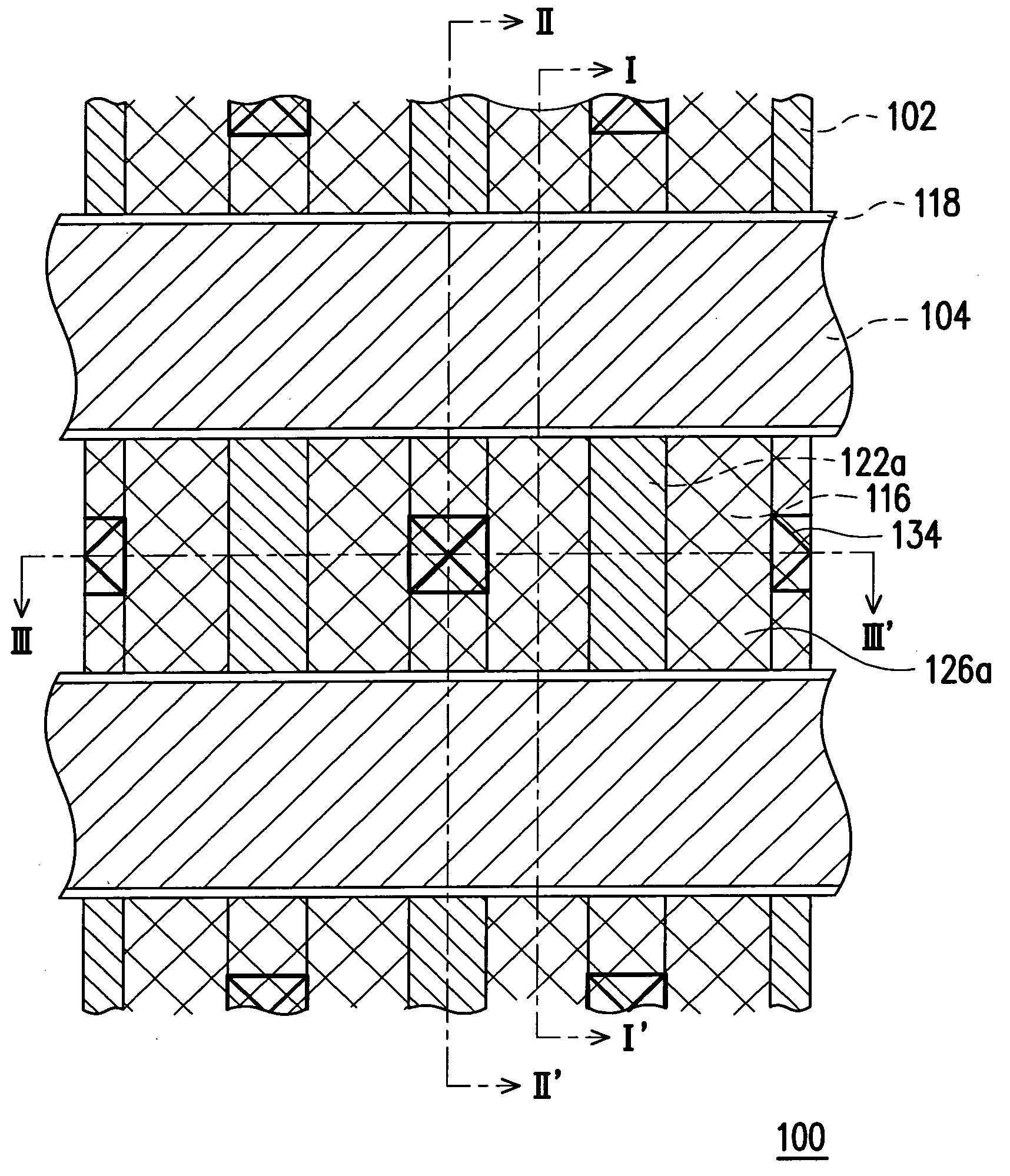
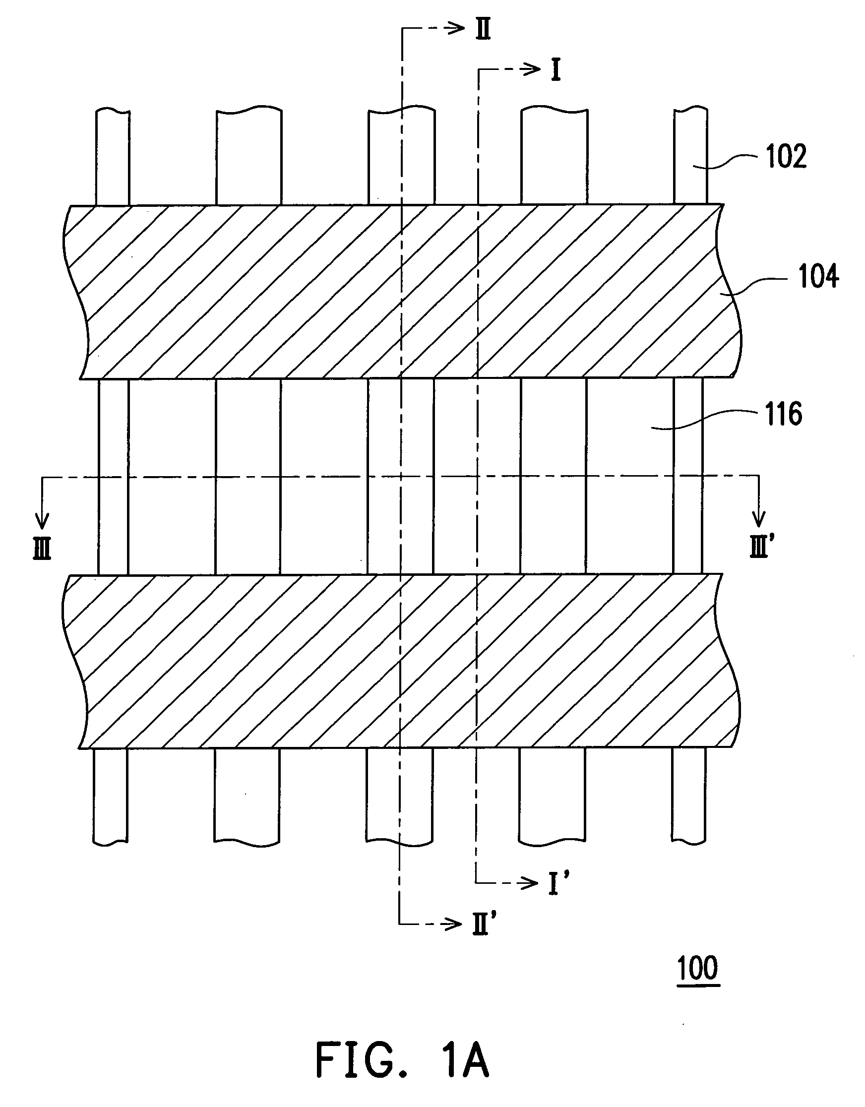
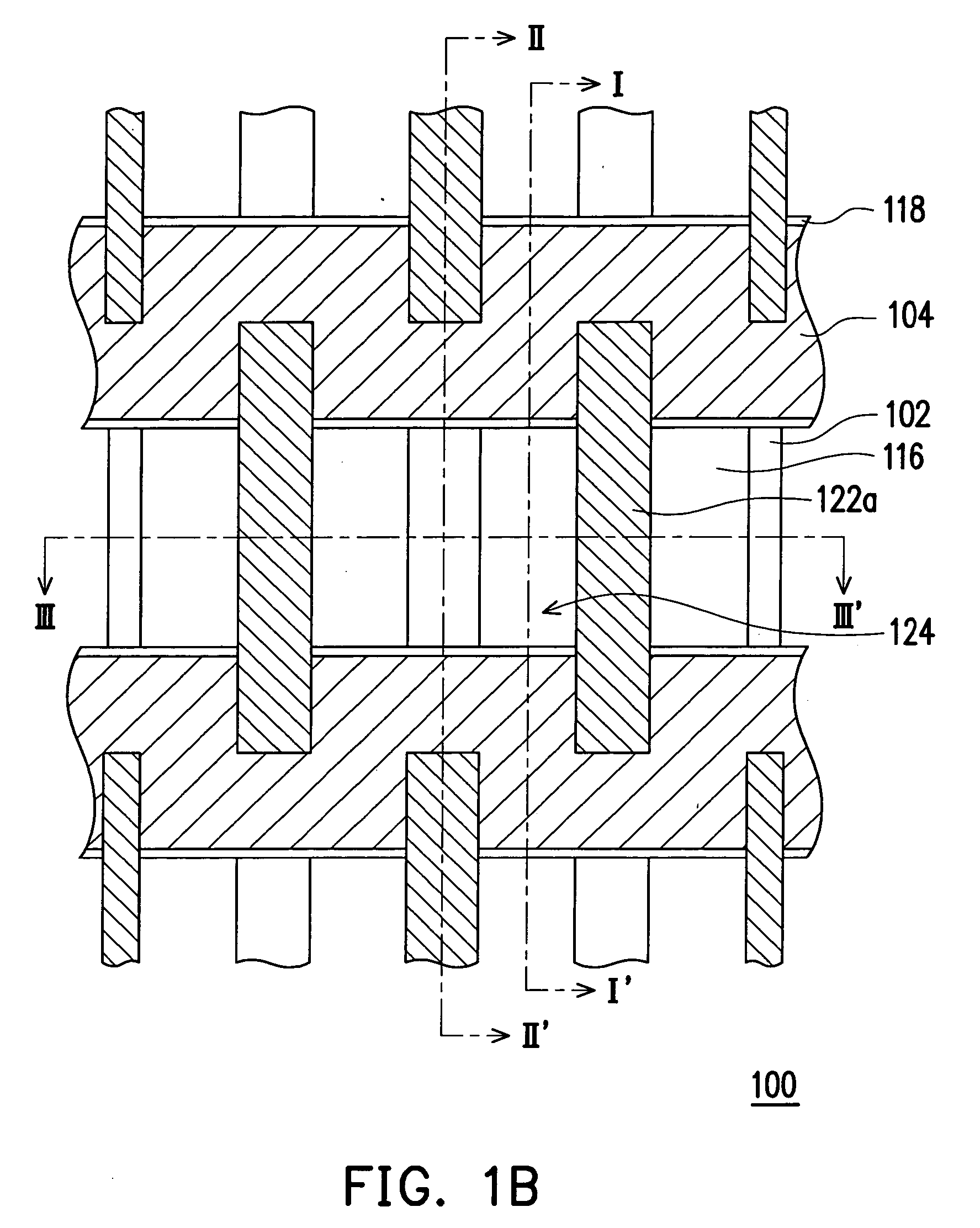
[0017]FIGS. 1A through 1C are top views showing the steps for fabricating a non-volatile memory according to one embodiment of the present invention; FIGS. 2A through 2D are schematic cross-sectional views along line I-I′ of FIG. 1A; FIGS. 3A through 3D are schematic cross-sectional views along line II-II′ of FIG. 1A; and FIGS. 4A through 4D are schematic cross-sectional views along line III-III′ of FIG. 1A.

[0018] First, as shown in FIGS. 1A, 2A, 3A and 4A, a substrate 100 is provided. The substrate 100 can be a silicon substrate. Then, a plurality of columns of isolation structures 102 are formed on the substrate 100. Wherein, isolation structures 102 are shallow trench isolation structures, for example, w...


PUM


Abstract

A method of fabricating a non-volatile memory is provided. A plurality of columns of isolation structures are formed on a substrate. A plurality of rows of stacked gate structures crossing over the isolation structures are formed on the substrate. A plurality of doping regions are formed in the substrate between two neighboring stacked gate structures. A plurality of stripes of spacers are formed on the sidewalls of stacked gate structures. A plurality of first dielectric layers are formed on a portion of the isolation structures adjacent to two rows of stacked gate structures. Also, one isolation structure is disposed between two neighboring first dielectric layers in the same row, while two neighboring rows comprising the first dielectric layer and the isolation structure are arranged in an interlacing manner. A plurality of first conductive: layers are formed between two neighboring first dielectric layers in the same row.

Description

BACKGROUND OF THE INVENTION [0001] 1. Field of the Invention [0002] The present invention relates to a memory device and fabricating method thereof. More particularly, the present invention relates to a non-volatile memory and fabricating method thereof. [0003] 2. Description of The Related Art [0004] Non-volatile memory is a type of memory that allows writing, reading and erasing data for multiple times, and the stored data will be retained even after power supplied to the device is off. Furthermore, non-volatile memory also has the advantages of small size, fast access speed and low power consumption. In addition, data can be erased in a block-by-block fashion so that the operating speed is further enhanced. With these advantages, non-volatile memory has become one of the most widely adopted memory devices for personal computers and electronic equipments. [0005] A typical non-volatile memory comprises an array of memory cells. The horizontally laid memory cells are serially connec...

Claims


Application Information

Patent Timeline
Patent Type & Authority Applications(United States)
IPC IPC(8): H01L21/336
CPCH01L21/28282H01L27/11568H01L27/115H01L29/40117H10B43/30H10B69/00
Inventor KIM, JONGOHWU, YIDERCHANG, KENT-KUOHUA
Owner MACRONIX INT CO LTD
Why Eureka
Try Eureka