Semiconductor memory device having COB structure and method of fabricating the same

Inactive Publication Date: 2005-03-08
SAMSUNG ELECTRONICS CO LTD
View PDF2 Cites 0 Cited by
  • Summary
  • Abstract
  • Description
  • Claims
  • Application Information

AI Technical Summary

Benefits of technology

It is an object of the present invention to provide a method for forming a semiconductor

Problems solved by technology

Moreover, A resistance between the storage electrode and the transistor is unfavorably high in a DRAM unit cells made by the first method compared to the second method.
This is because a misalignment problem, which is described in followings, is known to be more serious in the second method than in the first method.
However, the reduced distances may weaken immuni

Method used


Image

  • Semiconductor memory device having COB structure and method of fabricating the same
  • Semiconductor memory device having COB structure and method of fabricating the same
  • Semiconductor memory device having COB structure and method of fabricating the same

Examples


Embodiment Construction

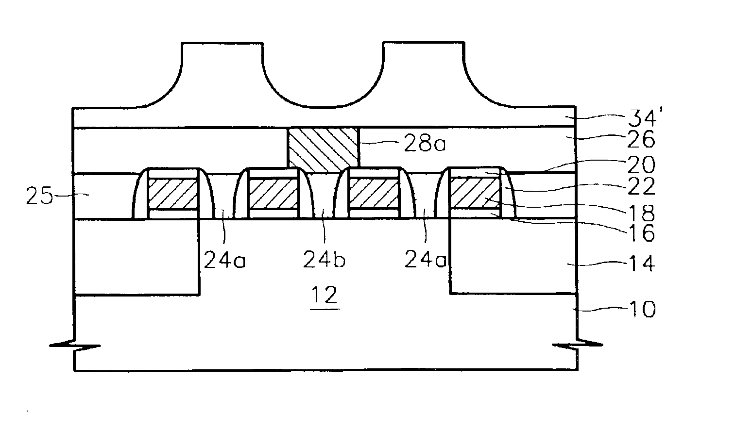
Preferred embodiments of the present invention will be described hereinafter with reference to the accompanying drawings, even though the scope of the present invention is not limited to the embodiments. In drawings, the geometrical magnitude of elements may be exaggerated for clarity. Like reference numerals in the drawings denote the same members.

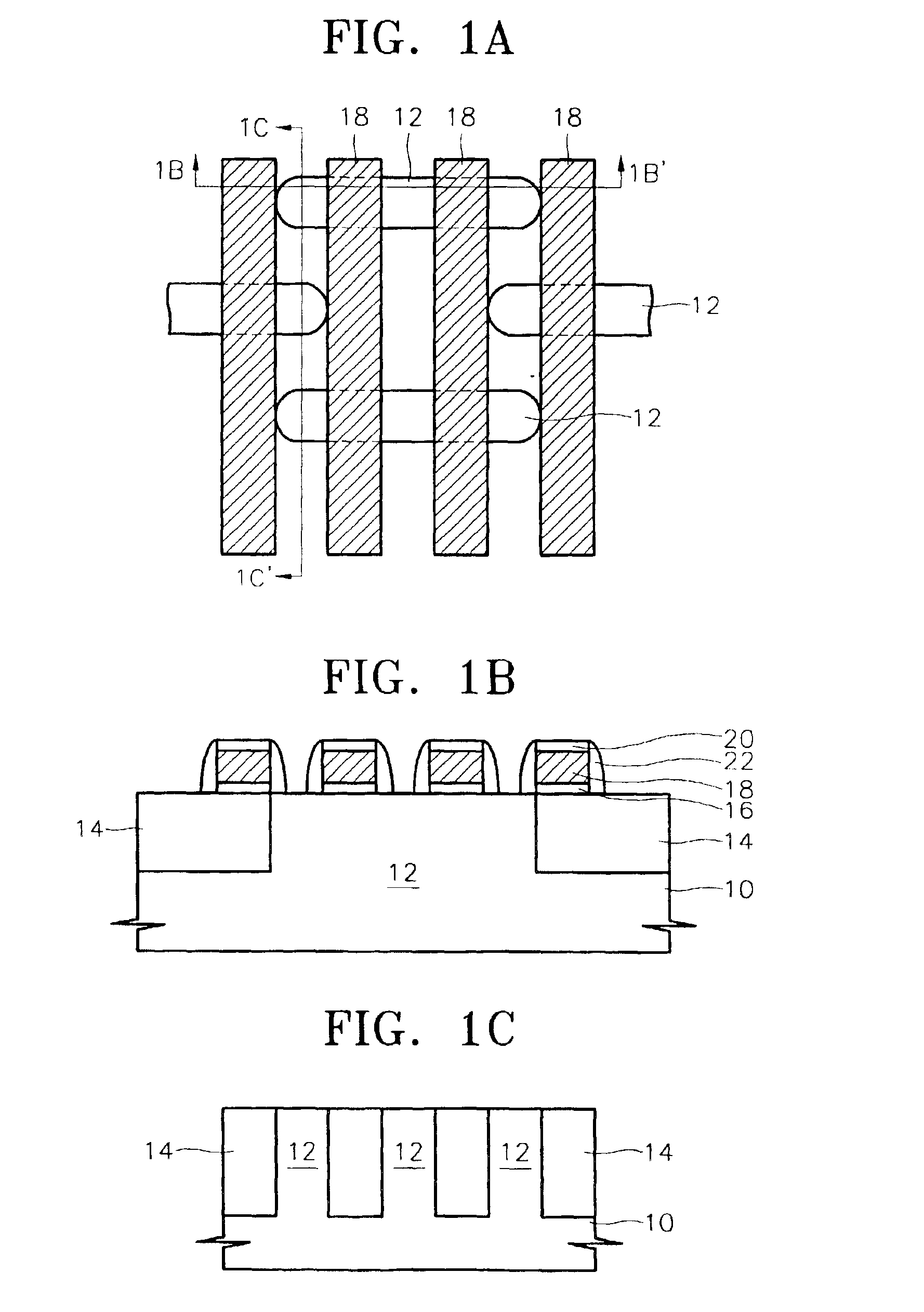
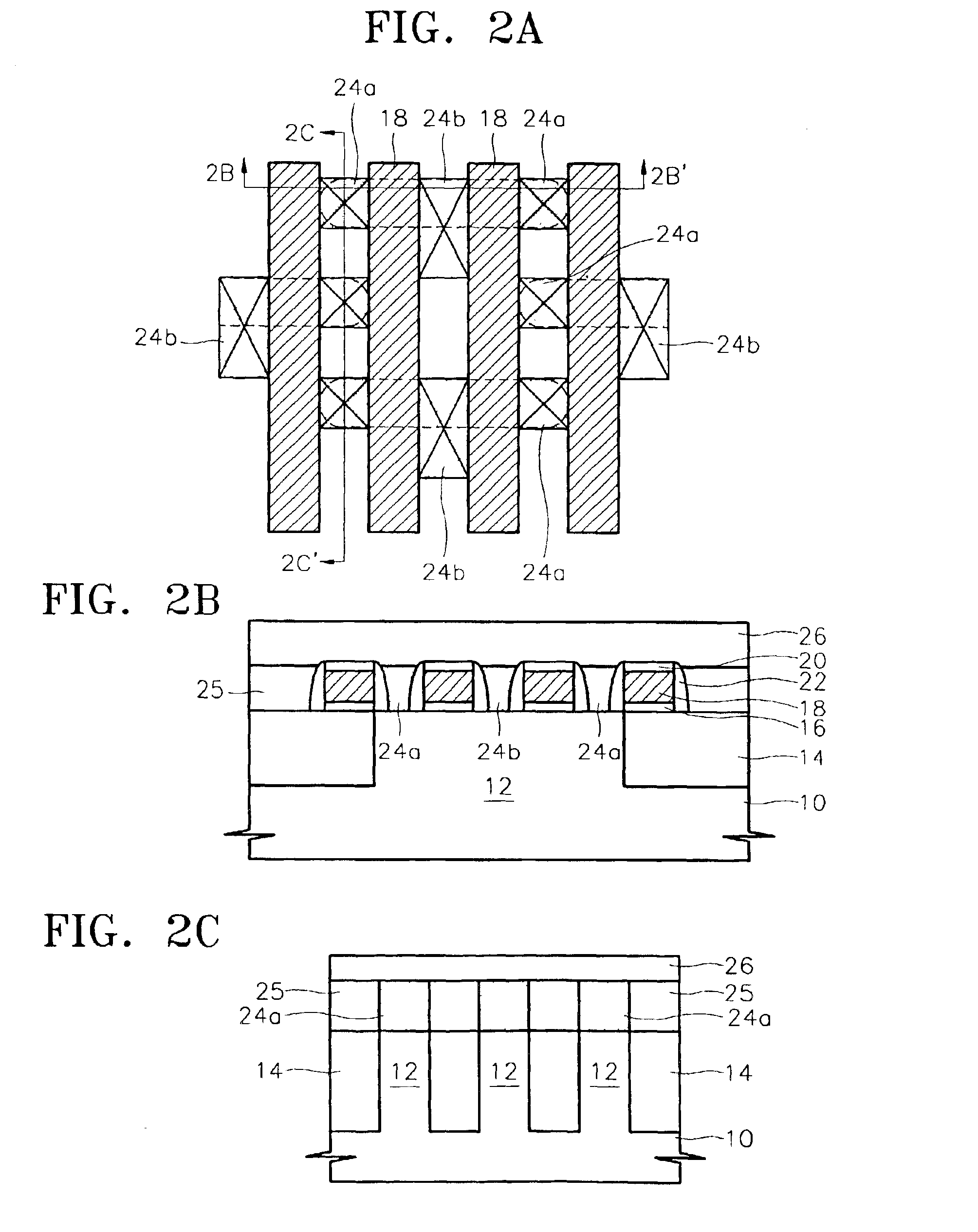
FIGS. 1a through 7a are schematic plan views illustrating successive process steps for forming a portion of a unit cell array in a DRAM device according to a preferred embodiment of the present invention. FIGS. 1b through 7b, 1c through 7c and 7d are cross-sectional views of the schematic plan views.

FIGS. 1b and 1c are cross-sectional views of FIG. 1a taken along a line 1B-1B′ and a line 1C-1C′ respectively. Referring to FIGS. 1a, 1b and 1c, an isolation region 14 is formed on a semiconductor substrate 10 by using trench technique, thereby defining active regions 12 in the substrate 10. The isolation region 14 may also be formed by using ...


PUM


Abstract

A fabrication method for forming a semiconductor device having COB (capacitor-over-bit line) structure is provided. A lower insulating film is formed on a substrate. Bit line patterns are formed on a portion of the lower insulating film. Each of the bit line patterns comprises a conductive bit line, a lower capping strip and an upper capping strip, which are sequentially stacked. Mask-defining layer is formed on the other portion of the lower insulating film. The upper capping strips are removed by wet etching technique to form a recess region. The lower capping strips and a portion of the mask-defining layer is etched isotropically to enlarge the recess region. An insulating mask is formed in the enlarged recess region. BC (buried contact) holes are formed substantially in self-aligned manner to the bit lines by using the mask as an etch mask. According to the present invention, the unfavorable electrical contact between the storage electrodes and the bit lines can be significantly relieved.

Description

This application relies for priority upon Korean Patent Application No. 2001-79690, filed on Dec. 15, 2001, the contents of which are herein incorporated by reference in their entirety.FIELD OF THE INVENTIONThe present invention relates to a semiconductor device and method of fabricating the same, and more specifically, to a dynamic random access memory (DRAM) device having capacitor-over-bit line (COB) structure and method of fabricating the same.BACKGROUND OF THE INVENTIONGenerally, a DRAM unit cell comprises a MOS transistor, a bit line and a storage capacitor. A storage electrode of the storage capacitor is electrically connected to a source electrode of the MOS transistor through a buried contact (BC) hole. The bit line is electrically connected to a drain electrode of the MOS transistor through a direct contact (DC) hole. In case of capacitor-over-bit line (COB) structure, the storage capacitor is formed over the bit line, and the BC hole is formed between the bit line of the ...

Claims


Application Information

Patent Timeline
IPC IPC(8): H01L21/70H01L21/02H01L21/60H01L21/8242H01L21/3205H01L27/108
CPCH01L21/76897H01L27/10855H01L28/90H10B12/0335H01L21/3205
Inventor PARK, BYUNG-JUN
Owner SAMSUNG ELECTRONICS CO LTD
Why Eureka
Try Eureka