Latchup prevention method for integrated circuits and device using the same

a technology of integrated circuits and latchups, applied in emergency protective circuit arrangements, transistors, etc., can solve the problems of parasitic scr inherent in the cmos process, logic errors or malfunctions of circuits, irreversible damage to ic, etc., to avoid latchup and minimize the influence of latchup trigger sources

Active Publication Date: 2007-05-22
WINBOND ELECTRONICS CORP
View PDF9 Cites 16 Cited by
  • Summary
  • Abstract
  • Description
  • Claims
  • Application Information

AI Technical Summary

Benefits of technology

[0011]It is therefore an object of the present invention to minimize the influence of latchup trigger sources, thereby avoiding latchup.

Problems solved by technology

Latchup effect is an important reliability issue in CMOS integrated circuit (IC), in which low impedance paths are formed by activation of a parasitic PNPN SCR (silicon controlled rectifier).
This results in logic errors or malfunctions of circuits, or even irreversible damage to the IC.
Unfortunately, because the P+ region of PMOS and N-well, P-sub and N+ regions of NMOS in integrated circuitry form a PNPN SCR structure, the parasitic SCR is inherent in CMOS process.
However, the most prominent is substrate current produced by hot carrier effect and / or forward biasing of parasitic diodes by noise appear on the pad during chip operation.
However, this increases process complexity and fabrication costs.
However, such solution requires large layout area and increases chip size, with utilization limited by specific layout restrictions.
While an alternative is to increase the distance between the I / O injector and internal circuit, this increases total chip size dramatically and is frequently limited in use.
This, however, also increases circuit complexity and layout space requirements.

Method used


Image

  • Latchup prevention method for integrated circuits and device using the same
  • Latchup prevention method for integrated circuits and device using the same
  • Latchup prevention method for integrated circuits and device using the same

Examples


Embodiment Construction

[0017]The present invention minimizes the influence of latchup trigger source, unlike conventional methods that prevent the occurrence of latchup in a passive way. In the present invention, current shunting diodes act as additional paths for substrate current to minimize the influence of latchup trigger source without modifying the original layout of the internal circuit and the ESD protection circuit, thereby avoiding of latchup.

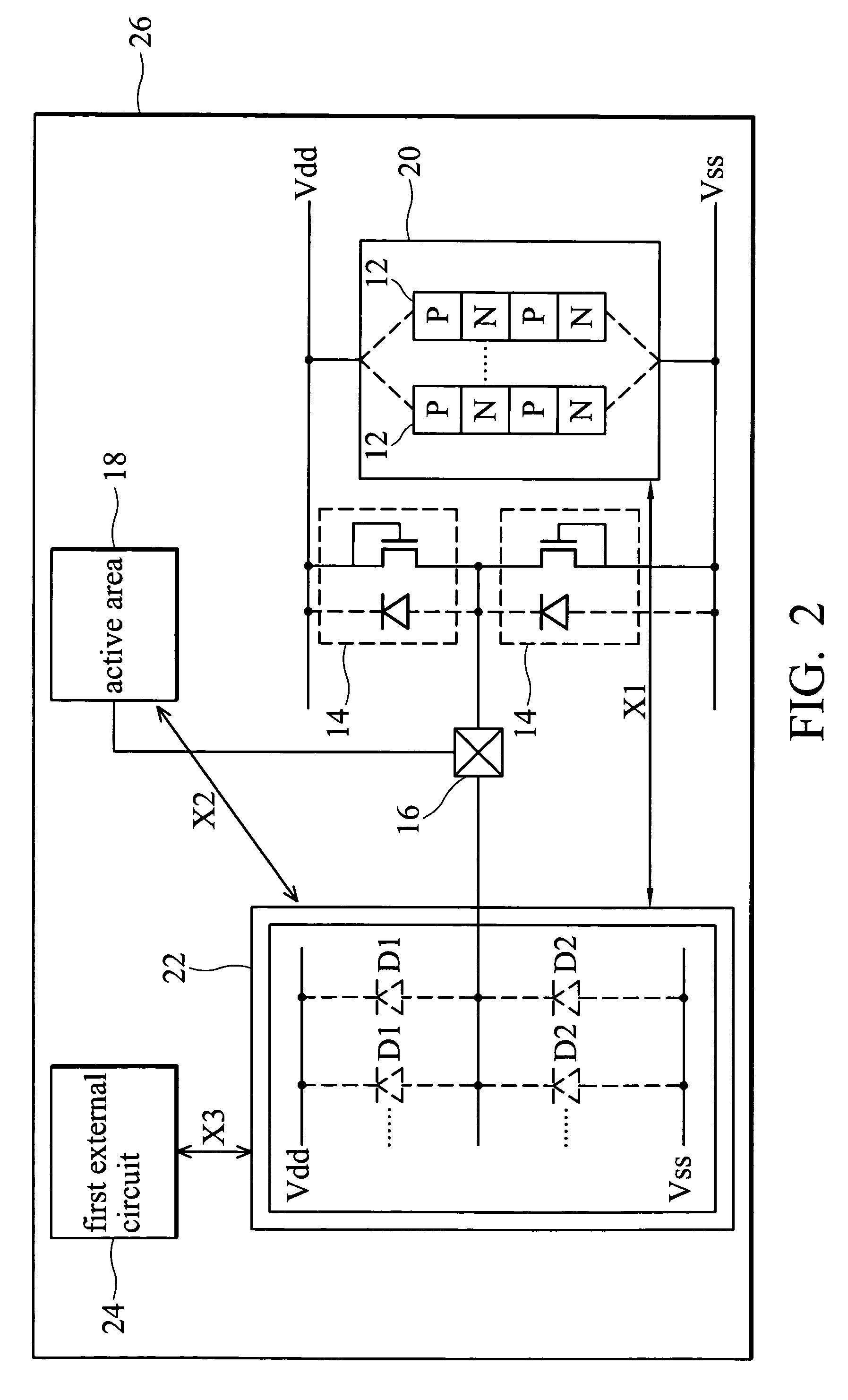
[0018]The latchup prevention method of the present invention is described as follows with reference to FIG. 2.

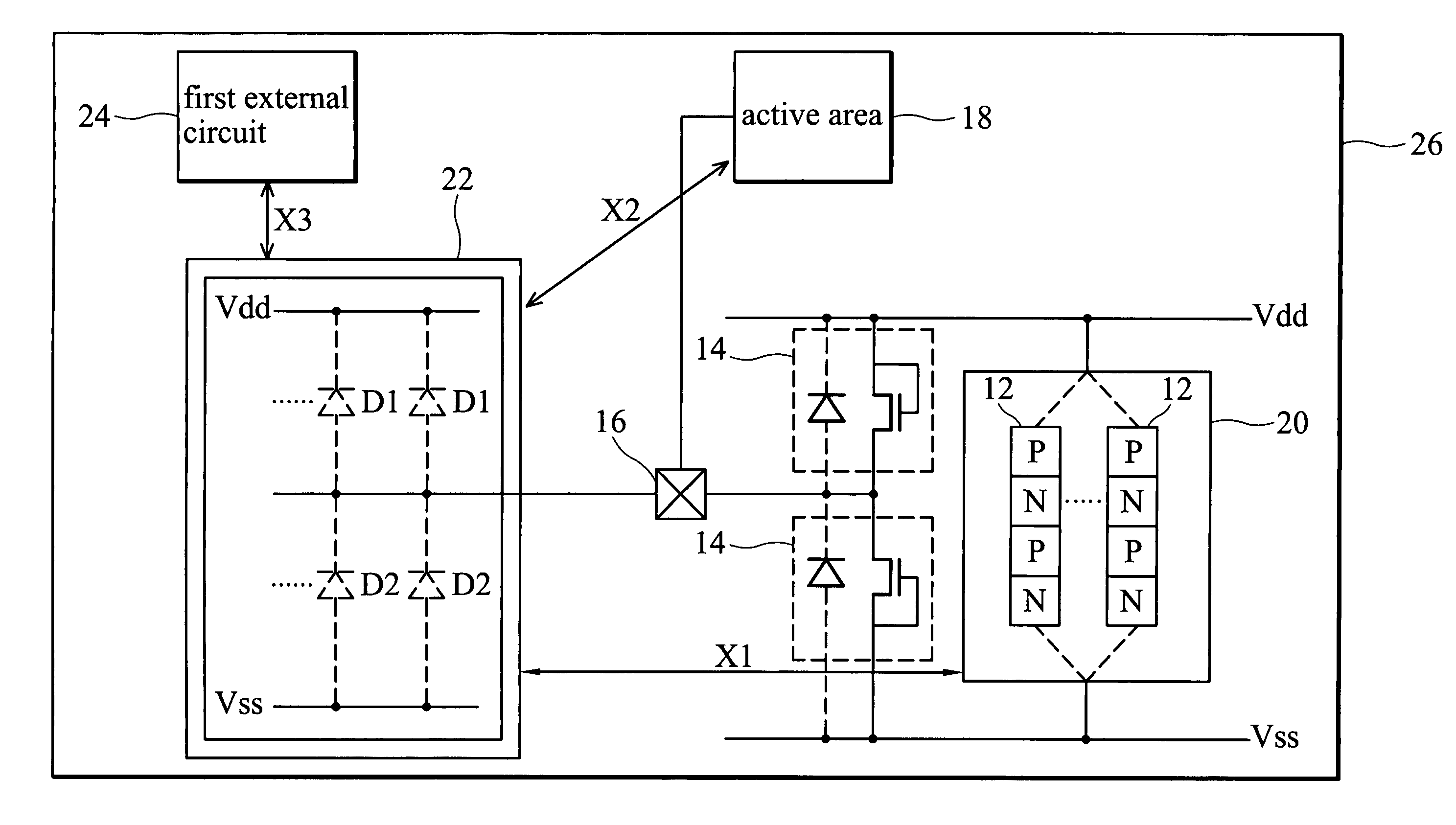
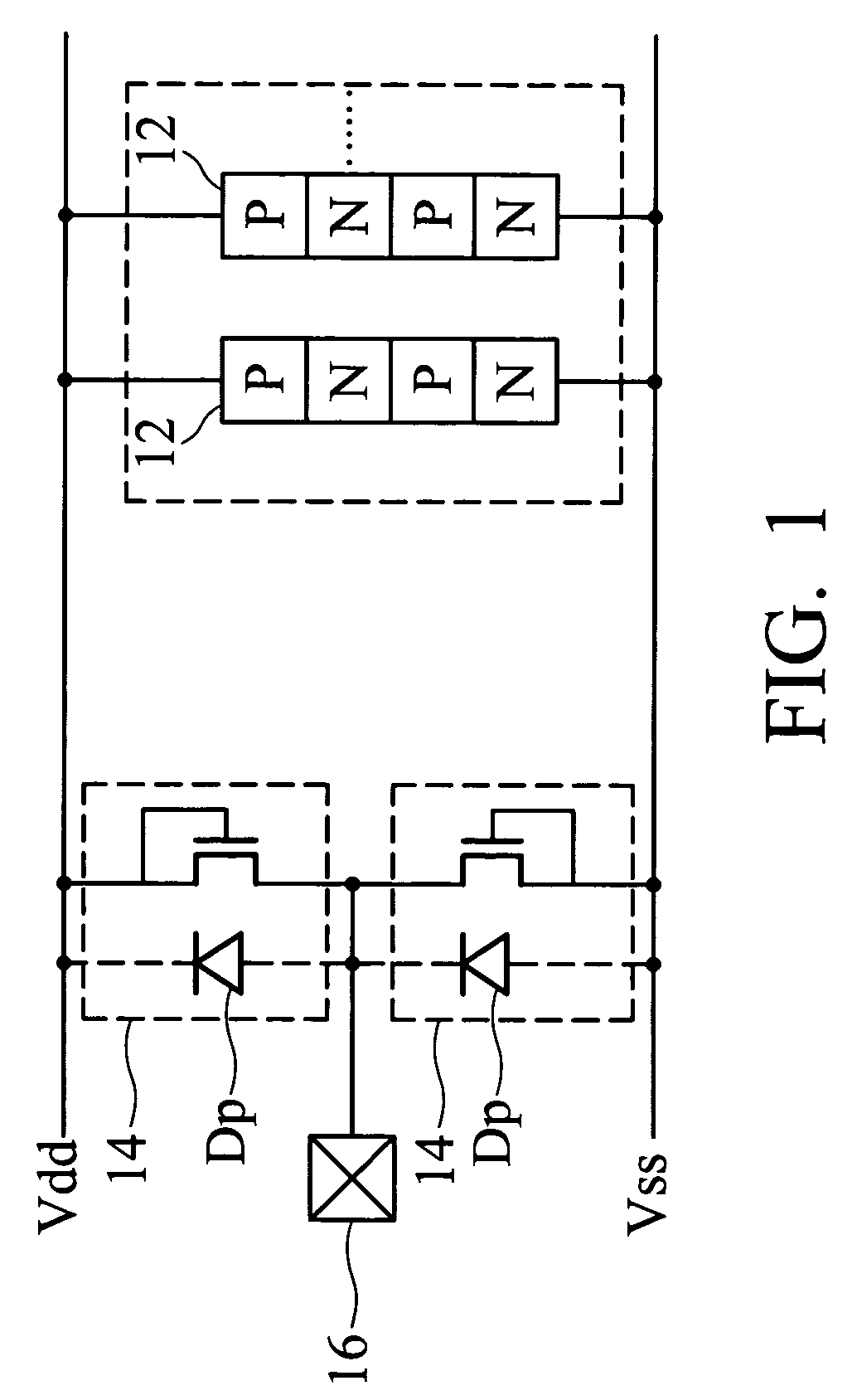
[0019]In the present invention, current shunting diodes (D1 and D2) are disposed on the substrate including an internal circuit 20, an active area 18, the first external circuit 24 and an ESD protection device 14, as shown in FIG. 2. The internal circuit 20 includes at least one parasitic SCR structure 12, and the active area 18 and the ESD protection device 14 coupled to the pad 16. Distance between the current shunting diodes (D1 and D2) and the i...


PUM


Abstract

An integrated circuit preventing latchup. In the integrated circuit, an internal circuit is disposed in a substrate and has a parasitic SCR structure. At least one ESD protection circuit and active area are disposed on the substrate and coupled to a pad. A first current shunting diode has an anode coupled to the pad and a cathode coupled to a first voltage source. A second current shunting diode has a cathode coupled to the pad and an anode coupled to a second voltage source. Minority-carriers guard rings surround the first current shunting diode and the second shunting diode. Distance between the first and second current shunting diodes and the internal circuit, the active area and the ESD protection circuit exceed 80 μm.

Description

BACKGROUND OF THE INVENTION[0001]1. Field of the Invention[0002]The present invention relates to integrated circuits, and more particularly, to a latchup prevention method for integrated circuits, and device using the same.[0003]2. Description of the Related Art[0004]Latchup effect is an important reliability issue in CMOS integrated circuit (IC), in which low impedance paths are formed by activation of a parasitic PNPN SCR (silicon controlled rectifier). Since the power supply has a low shunt impedance to ground during latchup, a large current occurs between the power supply and the ground. This results in logic errors or malfunctions of circuits, or even irreversible damage to the IC. Unfortunately, because the P+ region of PMOS and N-well, P-sub and N+ regions of NMOS in integrated circuitry form a PNPN SCR structure, the parasitic SCR is inherent in CMOS process.[0005]There are many origins and causes of latchup in CMOS. However, the most prominent is substrate current produced ...

Claims


Application Information

Patent Timeline
Patent Type & Authority Patents(United States)
IPC IPC(8): H02H9/00H01L27/02H01L27/06H01L27/092
CPCH01L27/0255H01L27/0629H01L27/0921
Inventor LIN, I-CHENG
Owner WINBOND ELECTRONICS CORP
Why Eureka
Try Eureka