

Semiconductor switching circuit for switching the paths of a high frequency signal in a mobile communications unit
a switching circuit and high frequency signal technology, applied in the field of semiconductor devices, can solve the problems of increasing insertion loss, deteriorating isolation, and difficult to secure communication lines for cellular phones of a single cellular phone system, so as to simplify the circuit configuration for controlling the terminals, improve isolation characteristics, and reduce the number of control terminals
- Summary
- Abstract
- Description
- Claims
- Application Information
AI Technical Summary
Benefits of technology
Problems solved by technology
Method used
Image

Examples
embodiment 1
(Embodiment 1)
[0042]A semiconductor apparatus will be discussed below according to Embodiment 1 of the present invention.
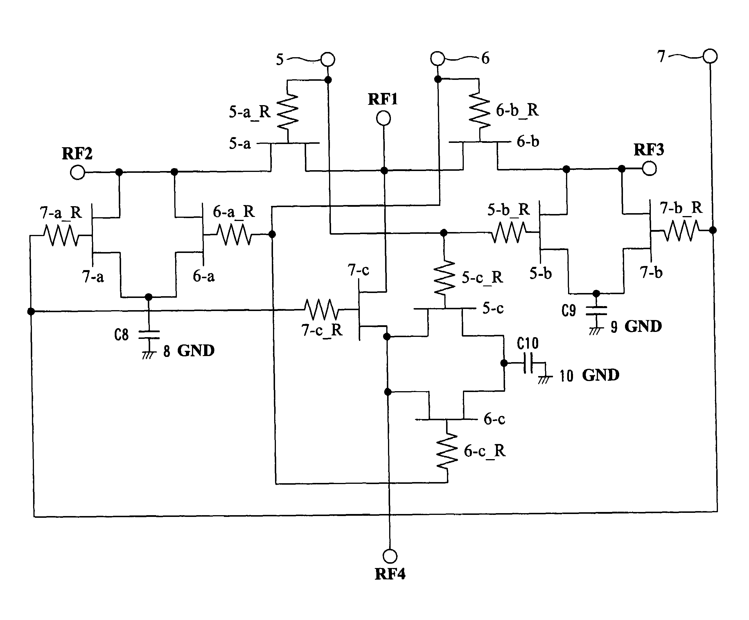
[0043]FIG. 1 is a circuit diagram showing the configuration of the semiconductor apparatus according to Embodiment 1. In this semiconductor apparatus, shunt FETs are basically configured so as to solve the foregoing problems. Control Logic serving as a control circuit for controlling on / off of through FETs and shunt FETs is not used.
[0044]In FIG. 1, reference numeral RF1 denotes an input terminal for inputting a high frequency signal, reference numerals RF2, RF3, and RF4 denote output terminals serving as high frequency ports for outputting high frequency signals, reference numerals 5, 6, and 7 denote gate bias terminals serving as control terminals, reference numerals 5-a, 6-b, and 7-c denote through FETs serving as through switch elements, reference numerals 5-a_R, 6-b_R, and 7-c_R denote gate resistors for controlling the through FETs, reference numerals 6-a, 7...
embodiment 2
(Embodiment 2)
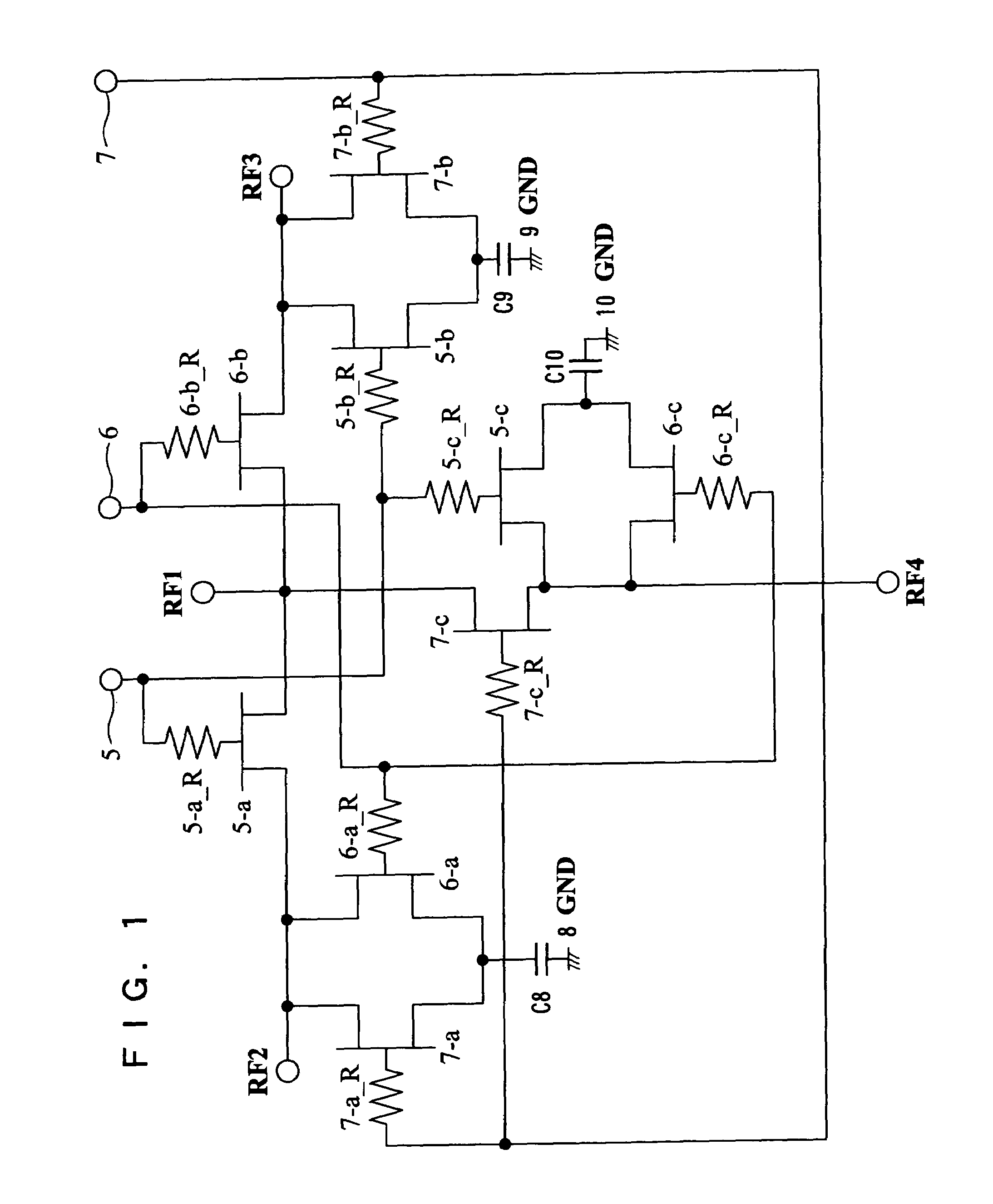
[0051]A semiconductor apparatus will be discussed below according to Embodiment 2 of the present invention.
[0052]FIG. 3 is a circuit diagram showing the configuration of the semiconductor apparatus according to Embodiment 2. In FIG. 3, reference numerals RF1 to RF4 denote first to fourth input / output terminals for inputting / outputting high frequency signals and reference numerals 5, 6, and 7 denote control terminals for inputting control signals. Reference numerals 5-g, 5-h, 5-i, 6-j, 6-k, 6-l, 7-m, 7-n, and 7-o denote switching elements which are FETs constituting a transfer circuit (hereinafter, referred to as “transfer FETs”) serving as a basic switch section. The n (n is an integer) FETs are connected in series in the transfer circuit. Reference numerals 5-j, 5-k, 5-l, 5-m, 5-n, 5-o, 6-g, 6-h, 6-i, 6-m, 6-n, 6-o, 7-g, 7-h, 7-i, 7-j, 7-k, and 7-l denote FETs for shunt circuits (hereinafter, referred to as “shunt FETs”). Reference numerals 5-i_R, 5-h_R, 5-g_R, 5-j_R,...
embodiment 3
(Embodiment 3)
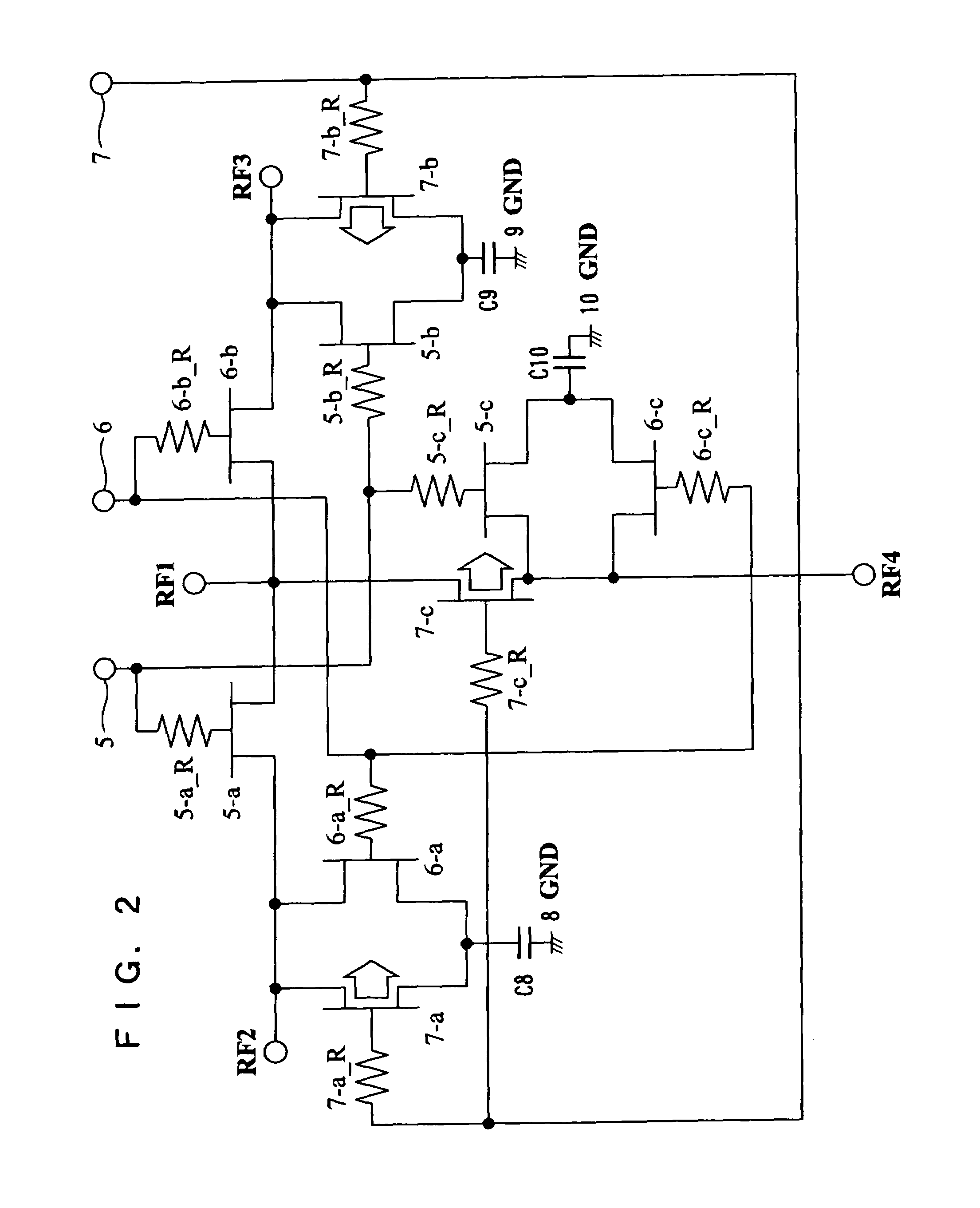
[0062]A semiconductor apparatus will be discussed below according to Embodiment 3 of the present invention.
[0063]FIG. 4 is a circuit diagram showing the configuration of the semiconductor apparatus according to Embodiment 3. In FIG. 4, reference numerals RF1 to RF4 denote first to fourth input / output terminals for inputting / outputting high frequency signals and reference numerals 5, 6, and 7 denote control terminals for inputting control signals. Reference numerals 5-d, 6-e, and 7-f denote switching elements which are multigate transfer FETs for a transfer circuit serving as a basic switch section. Reference numerals 5-e, 5-f, 6-d, 6-f, 7-d, and 7-e denote shunt FETs for shunt circuits. Reference numerals 5-d_R1, 5-d_R2, 5-d_R3, 5-e_R1, 5-e_R2, 5-e_R3, 5-f_R1, 5-f_R2, 5-f_R3, 6-d_R1, 6-d_R2, 6-d_R3, 6-e_R1, 6-e_R2, 6-e_R3, 6-f_R1, 6-f_R2, 6-f_R3, 7-d_R1, 7-d_R2, 7-d_R3, 7-e_R1, 7-e_R2, 7-e_R3, 7-f_R1, 7-f_R2, and 7-f_R3 denote gate resistors.
[0064]The following will di...
PUM
 Abstract
Description
Claims
Application Information