Semiconductor force sensor

a technology of magnetic field and sensor, which is applied in the direction of force measurement using piezo-resistance materials, instruments, liquid/fluent solid measurement, etc., can solve the problems of inability to accurately measure the force applied in the direction orthogonal to the diaphragm section, inability to accurately measure the force applied in the direction orthogonal to the thin plate, and inability to expand the operating temperature range of the case main body. , to achieve the effect of easy formation,

Active Publication Date: 2007-06-26
HOKURIKU ELECTRIC INDS
View PDF14 Cites 23 Cited by
  • Summary
  • Abstract
  • Description
  • Claims
  • Application Information

AI Technical Summary

Benefits of technology

[0010]When the through hole in the opposed wall section is formed as in the present invention and a force in the direction orthogonal to the diaphragm section is applied to the sphere, the diagram section warps due to the force applied to the sphere. On contrast therewith, when a force in a direction other than the direction orthogonal to the diaphragm section is applied to the sphere, the sphere rotates on the central portion of the diaphragm section due to a component force. Application of an undue force to the diaphragm section thus can be prevented. For this reason, breakage of the diaphragm section can be prevented. Further, only the component of the force applied to the direction orthogonal to the diaphragm section can be accurately measured.
[0020]The semiconductor force sensor according to the present invention can be applied to a surface-mount type semiconductor force sensor. If it is applied to the surface-mount type semiconductor force sensor, the surface-mounting area of the semiconductor force sensor can be reduced. In addition, there is an advantage that no terminals are bent due to an external force, or the like.

Problems solved by technology

In such a semiconductor force sensor, however, when a force in a direction other than a direction orthogonal to the diaphragm section is transmitted to the diaphragm section through the sphere, an undue force is applied to the diaphragm section, so that the diaphragm section might be broken.
Further, a force applied to the direction orthogonal to the diaphragm section could not be measured accurately.
Then, there was a problem that the force applied to the direction orthogonal to the thin plate could not be accurately measured.

Method used


Image

  • Semiconductor force sensor
  • Semiconductor force sensor
  • Semiconductor force sensor

Examples


first embodiment

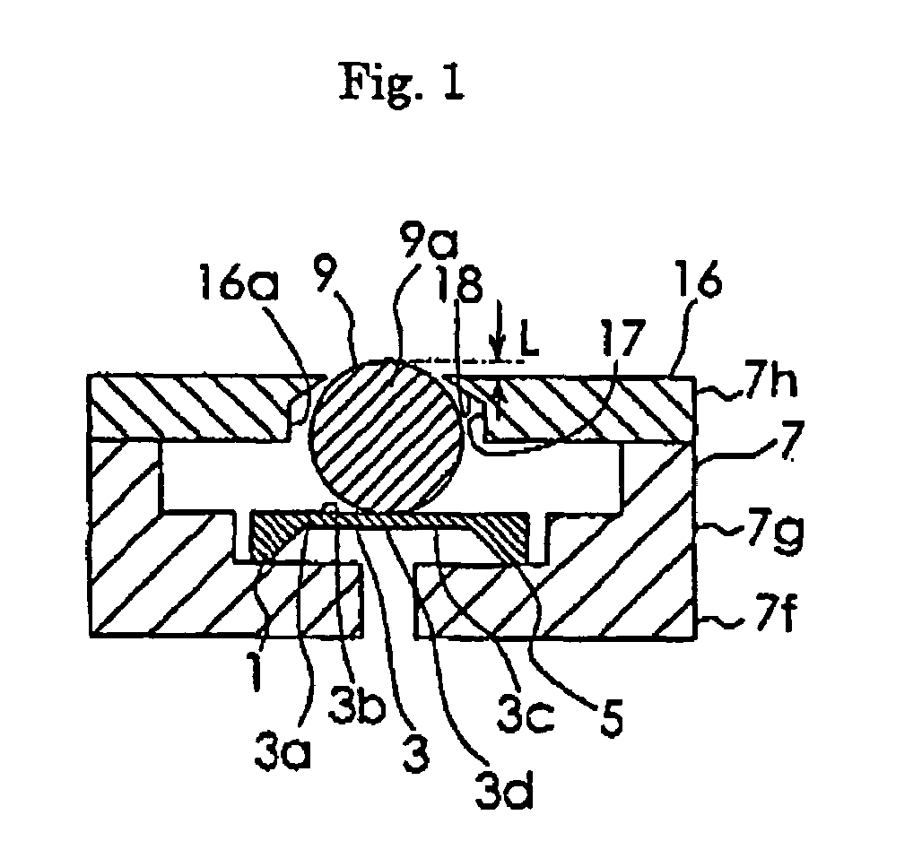
[0027]Embodiments of the present invention will be described in detail with reference to the accompanying drawings. FIG. 1 is a schematic sectional view of a semiconductor force sensor according to the present invention. Referring to FIG. 1, a semiconductor force sensor element 1 is formed using a Silicon semiconductor substrate with an area of 2.3 mm square and a thickness of 300 μm, for detecting a force. At the center of the semiconductor substrate is formed a diaphragm section 3, and its periphery is supported by a base section 5 integral with the diaphragm section 3. The diaphragm section 3 has a converting section 3a on its front surface portion 3b. The converting section 3a comprises four diffusion resistances constituting a bridge circuit formed in the semiconductor substrate. The diffusion resistances convert a force applied to the converting section 3a into an electric signal by piezoresistive effect. The diaphragm section 3 is a silicon diaphragm constituted by the bottom...

third embodiment

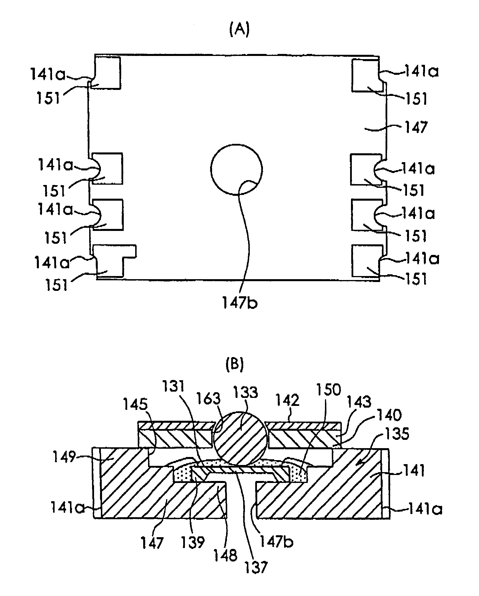
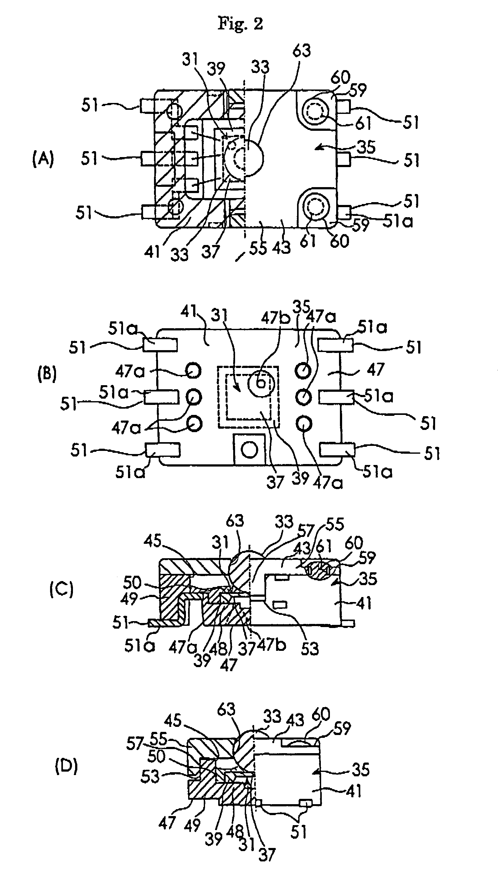
[0039]FIGS. 4(A) and 4(B) are a back view and a sectional view of a semiconductor force sensor according to the present invention applied to a surface mounted type semiconductor force sensor. This embodiment includes the same structure as the semiconductor force sensor shown in FIG. 2, except for the structure of the case. Accordingly, in this drawing, reference numerals added by 100 are assigned to the members that are the same as those of the semiconductor force sensor in FIG. 2, and their descriptions will be thereby omitted.

[0040]As shown in these figures, a case 135 includes a case main body 141 and a lid member 143 fixed to the case main body 141. The case main body 141 is formed of ceramics and has a shape of a box having an opening 145 in one surface thereof. This case main body 141 includes a bottom wall section 147 and a peripheral wall section 149 integrally formed with the peripheral edge portion of the bottom wall section 147. On the back surface of the bottom wall sect...


PUM

PropertyMeasurementUnit
thicknessaaaaaaaaaa
diameteraaaaaaaaaa
diameteraaaaaaaaaa

Abstract

A semiconductor force sensor capable of preventing a diaphragm part (37) from being broken and accurately measuring a force applied thereto in a direction orthogonal to the diaphragm part (37), wherein a force transmitting means for applying a measured force to the diaphragm part (37) of a semiconductor force sensor element (31) is formed of a sphere (33) having a rigidity, and a through hole (63) passing through an opposed wall part (55) toward the diaphragm (37) is formed in the opposed wall parts (55) at a position opposed to the center part of the diaphragm part (37) so that a part of the sphere (33) can face the outside of the opposed wall part (55) and stores a part of the remaining part of the sphere (33) to allow the sphere (33) to be moved only in a direction orthogonal to the diaphragm part (37) and rotated on the center part of the diaphragm part (37).

Description

TECHNICAL FIELD[0001]The present invention relates to a semiconductor force sensor for detecting a force such as a pressure or the like by a semiconductor force sensor element, for output as an electric signal.BACKGROUND ART[0002]Japanese Patent Application Laid-Open Publication No. 118935 / 1993 discloses a semiconductor force sensor including a semiconductor force sensor element having a diaphragm section and a sphere for transmitting a force to the diaphragm section. The semiconductor force sensor warps the diaphragm section by the force applied to the sphere and converts a change in this force to an electric signal, thereby measuring the force applied to the sphere or turning on or off a switch. In the semiconductor force sensor, a recess section, in which the sphere is placed, is formed in the central portion of the semiconductor force sensor element, and a through hole, into which the sphere to fitted, is formed in the opposed wall section of an receiving case facing the recess ...

Claims


Application Information

Patent Timeline
Patent Type & Authority Patents(United States)
IPC IPC(8): G01B7/16G01L1/18H01L29/84
CPCG01L1/18G01L1/2231
Inventor HIROSE, SHIGERUSAWAMURA, HIROYUKIANDO, MASATOMOTOKI, YOSHIMITSU
Owner HOKURIKU ELECTRIC INDS
Why Eureka
Try Eureka