Wafer carrier for growing GaN wafers

gans, which is applied in the direction of crystal growth process, chemically reactive gases, coatings, etc., can solve the problems of inability to meet the requirements of gan wafers, non-uniform temperature, and inferior quality of the layer(s) deposited along the peripheral portion of the wafer. , to achieve the effect of improving the quality of the resultant semiconductor wafers, and reducing the quality a gan wafer carrier and gan wafers, a gan wafer carrier and gan wafers, a gan wafer carrier and gan wafers, a technology of gan wafers, a technology which is applied in the field of gan wafers, which is applied the quality of gan wafers, and the application in the a gan wafer carrier and gan wafer carrier and gan wafer carrier and gan wafer carrier and gan wafer carrier and gan wafers, which is applied in the field of gan wafers, which is applied in

Inactive Publication Date: 2007-06-26
VEECO INSTR
View PDF38 Cites 47 Cited by
  • Summary
  • Abstract
  • Description
  • Claims
  • Application Information

AI Technical Summary

Benefits of technology

[0016]The present invention seeks to overcome the problems that occur with certain prior art apparatus. Specifically, in prior art apparatus, a susceptor is used to support the wafer carrier. The susceptor is typically positioned between the wafer carrier and heating filaments used to heat the wafer carrier. According to those skilled in the art, the susceptor captures heat from the heating filament which requires the heating filament to be heated to a higher temperature to produce the same wafer temperature. This is due to the susceptor drawing some of the heat and preventing direct heat transfer from the heating filament to the wafer carrier. The present invention overcomes this problem by eliminating the need for the susceptor through the use of a specially designed wafer carrier directly coupled with an upper end of a spindle.
[0021]Thus, the present application solves at least two problems when growing epitaxial layers. One problem solved, which was addressed in above-mentioned U.S. application Ser. No. 09 / 619,254 filed Jul. 19, 2000, the disclosure of which is hereby incorporated by reference herein, is that the vacuum drawn through the porous discs prevents the edges of the wafers from warping. The other problem solved is that the specially designed wafer carrier may be used in an apparatus having no object between the wafer carrier and the heating filament for better heat transfer between the heating filament and the wafer carrier. As a result, the heating filament does not have to be heated to extremely high temperatures (e.g. 2,500–2,600° C.). This is particularly beneficial for growing GaN wafers which must be grown at particularly high temperatures.
[0023]The deposition chamber may also include a pump in communication with a spindle opening that generates a vacuum or suction within an elongated opening extending through the spindle. Upon generating the area of low pressure within the spindle opening, a vacuum or low-pressure area of equal force is generated within both the central opening and the hollow shafts of the wafer carrier. When wafers are positioned atop the porous discs of the wafer carrier and one or more reactant gases are introduced into the reaction chamber, the vacuum or suction within the central opening of the wafer carrier is less than the pressure level within the reaction chamber. As a result, suction develops at an interface between the wafer and the porous discs. Such suction prevents the peripheral edges of the wafers from warping or pulling away from the wafer carrier as the epitaxial layers are deposited, as occurs in prior art deposition chambers (e.g., the prior art embodiment shown in FIG. 1A). As a result, uniform epitaxial layers are formed across the entire surface of the wafer, thereby providing reliable semiconductor devices that may be harvested from the peripheral regions of the wafers.

Problems solved by technology

Unfortunately, this temperature difference diminishes the quality of the resultant semiconductor wafers.
For example, the higher temperature of the wafer carrier surface results in a nonuniform temperature on the surface of the wafers, particularly along their outer periphery, such that the layer(s) deposited along peripheral portions of wafers ordinarily are of inferior quality and limited value.
Moreover, arrangements using a susceptor require too much filament power to heat the susceptor which then heats the wafer carrier.
Moreover, there is uneven heating of the wafers because the interior portions of the wafers are being heated when the curled outer portions of the wafers are further away from the heating assembly as a result of this wafer warpage.
As a result, the epitaxial layers are not uniform across the wafers and the outer portions of the warped wafers 10 must be discarded.
Another problem with the arrangement shown in FIGS. 1A and 1B is that the susceptor 14 prevents efficient heating of the wafer carrier 12.
This situation is problematic when relatively high temperatures must be attained, such as when growing GaN wafers.

Method used


Image

  • Wafer carrier for growing GaN wafers
  • Wafer carrier for growing GaN wafers
  • Wafer carrier for growing GaN wafers

Examples


Embodiment Construction

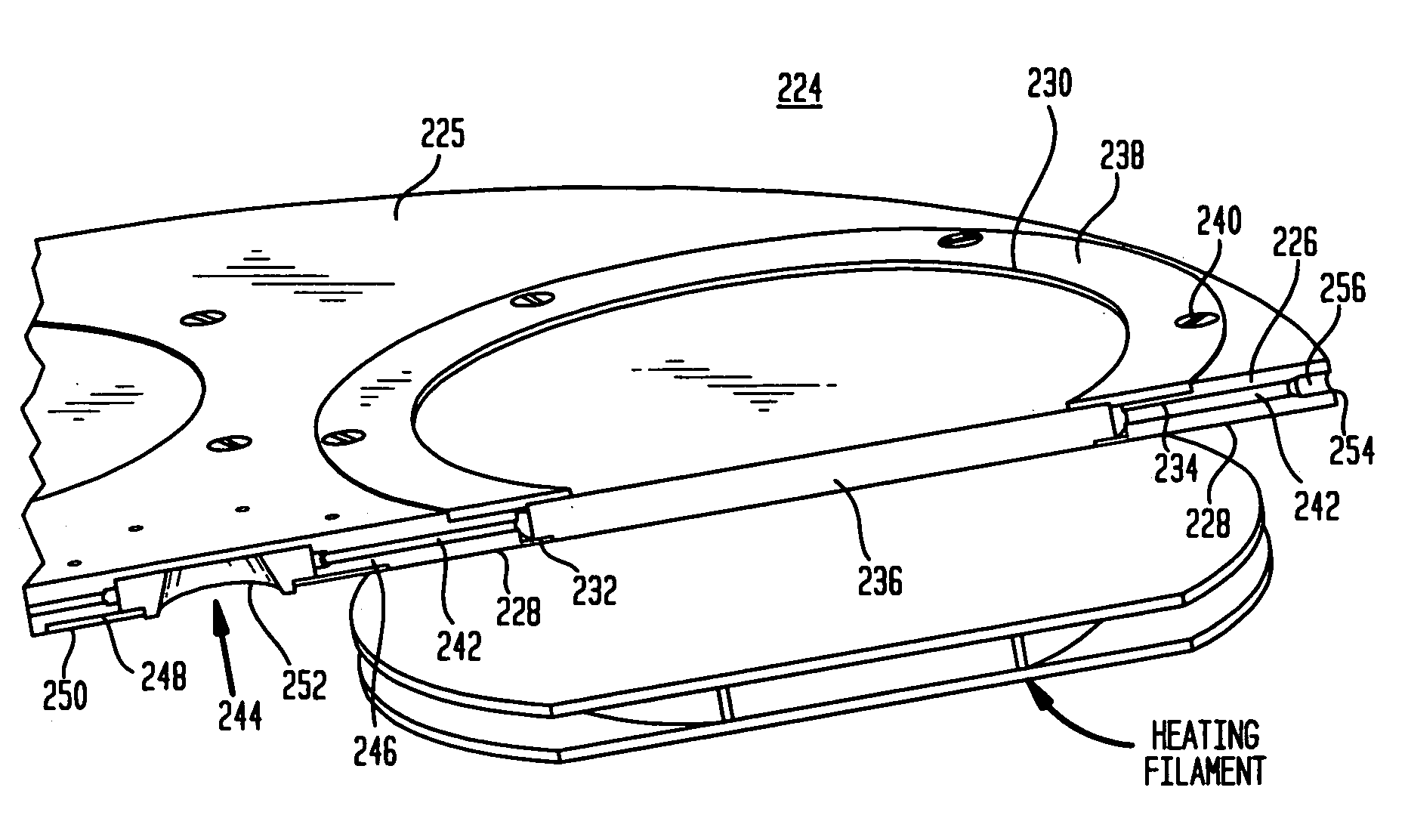
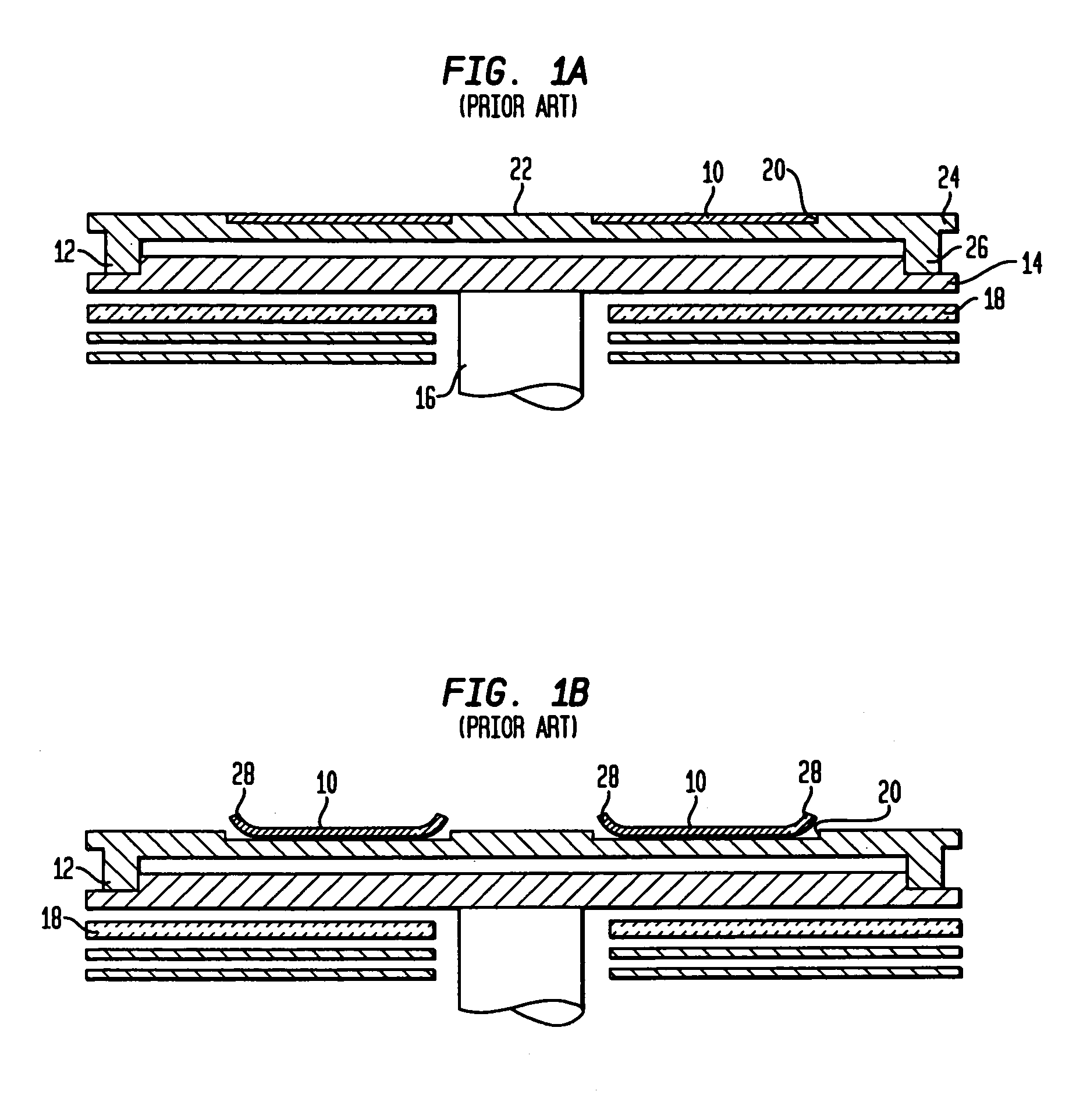
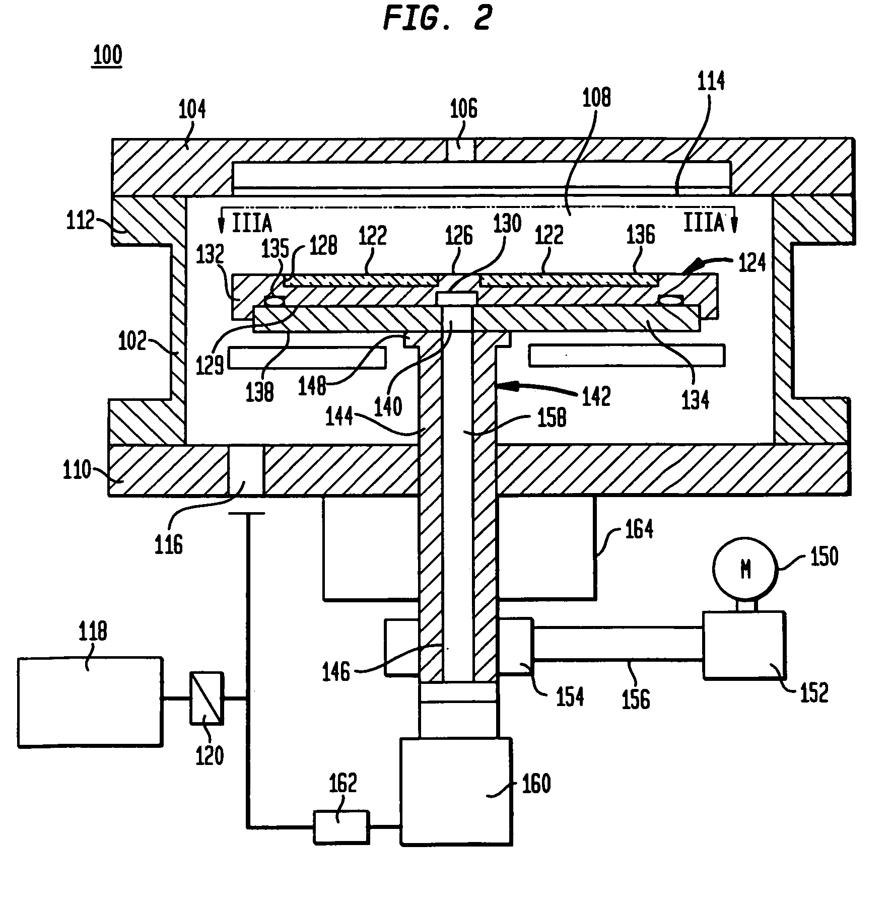
[0038]FIG. 2 shows an apparatus for growing epitaxial layers on wafers. The apparatus includes a deposition chamber 100 comprising a side wall 102, and a top flange 104 including one or more openings 106 for introducing reactant chemicals, such as reactant gases, into an interior region 108 of deposition chamber 100. Deposition chamber 100 also includes a bottom-sealing flange 110. The deposition chamber 100 is made of stainless steel with the top and bottom flanges 104 and 110 being sealingly engaged with sidewall 102. The reactant gases introduced through the opening 106 in top flange 104 are generally uniformly distributed by one or more showerheads 114. The reactant gases interact with one another inside deposition chamber 100 to form epitaxial layers upon wafers. After the reactant gases interact with one another and are deposited atop wafers, the waste material is removed through an exhaust 116 extending through bottom-sealing flange 110. In certain embodiments, the waste reac...


PUM

PropertyMeasurementUnit
porosityaaaaaaaaaa
temperatureaaaaaaaaaa

Abstract

A wafer carrier for growing wafers includes a plate having a first surface and a second surface, a plurality of openings extending from the first surface to the second surface of the plate, and a porous element disposed in each of the plurality of openings, each porous element being adapted to support one or more wafers. The wafer carrier also has a blind central opening extending from the second surface toward the first surface of the plate, and a plurality of shafts extending outwardly from the blind central opening. Each shaft has a first end in communication with the blind central opening and a second end in communication with one of the porous elements for providing fluid communication between the blind central opening and one of the porous elements. Suction is formed at a surface of each porous element by drawing vacuum through the blind central opening and the shafts.

Description

CROSS REFERENCE TO RELATED APPLICATIONS[0001]This application claims the benefit of the filing date of U.S. Provisional Patent Application No. 60 / 514,959 filed Oct. 28, 2003, the disclosure of which is hereby incorporated herein by reference.BACKGROUND OF THE INVENTION[0002]The present invention relates to making semiconductor materials and devices and more particularly relates to an apparatus for growing epitaxial layers for materials such as GaN.[0003]Semiconductor wafers are frequently manufactured by placing wafers (also known as substrates) within a reaction chamber of a chemical vapor deposition (CVD) reactor and then growing one or more epitaxial layers on the wafers. During this process, wafers are placed inside the CVD reactor and reactant chemicals in gaseous form are introduced over the wafers in controlled quantities and at controlled rates for growing epitaxial layers on the wafers.[0004]CVD reactors have various designs, including horizontal reactors in which wafers ar...

Claims


Application Information

Patent Timeline
Patent Type & Authority Patents(United States)
IPC IPC(8): C23C16/00C23C16/458C30B25/12C30B31/14
CPCC23C16/4585C30B25/12C30B31/14
Inventor BOGUSLAVSKIY, VADIMGURARY, ALEXSTALL, RICHARD A.
Owner VEECO INSTR
Why Eureka
Try Eureka