
Device having electronic components mounted therein and method for manufacturing such device

a technology of electronic components and devices, which is applied in the direction of electrical apparatus construction details, electrical apparatus casings/cabinets/drawers, instruments, etc., can solve problems such as device malfunction, and achieve the effect of preventing direct heat transfer from the first electronic component to the second electronic componen

Active Publication Date: 2012-02-21
NEC PLATFORMS LTD
View PDF13 Cites 0 Cited by
  • Summary
  • Abstract
  • Description
  • Claims
  • Application Information

AI Technical Summary

Benefits of technology

[0011]The object of the present invention is to provide a device having electronic components mounted therein and a manufacturing method thereof wherein electronic components that generate a large amount of heat and electronic components that have a high necessity of being thermally protected can be stacked.
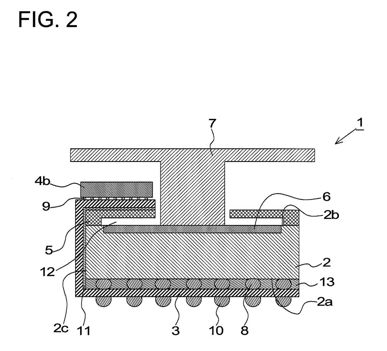
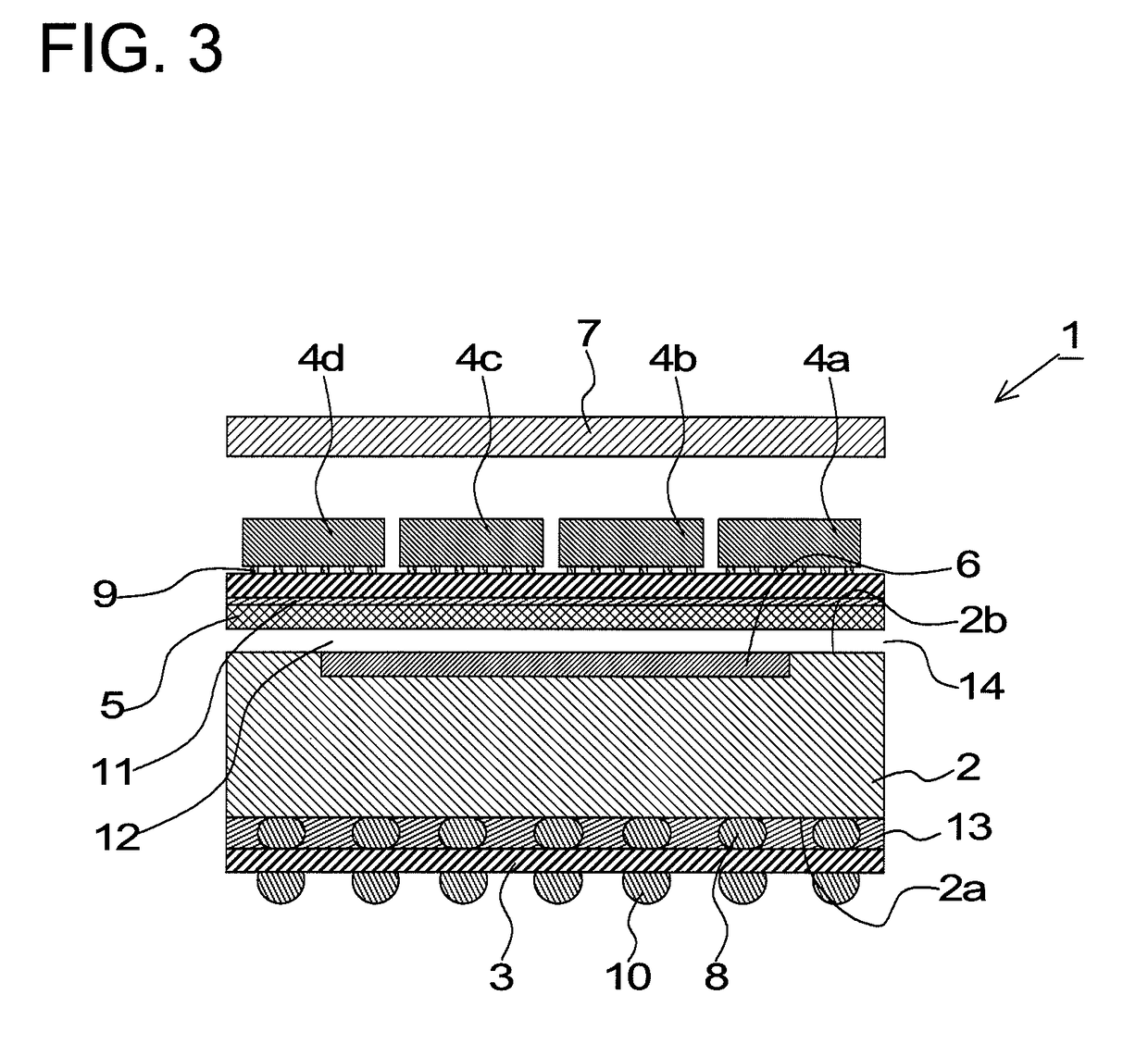
[0012]According to a first aspect of the present invention, there is provided a device having electronic components mounted therein. The device has a first electronic component having an external terminal on a first surface and a heat spreader on a second surface and at least one second electronic component that is located in the direction of the second surface of the first electronic component. The device has a flexible circuit board that is electrically connected to the external terminal of the first electronic component and at least one second electronic component. At least the part of the flexible circuit board to which at least one second electronic component is connected is located on the second surface side of the first electronic component. The device has a spacer that prevents direct heat transfer between at least part of the flexible circuit board and the second surface of the first electronic component.
[0013]According to a second aspect of the present invention, there is provided a manufacturing method for a device having electronic components mounted therein. The method has installing a spacer on a second surface of a first electronic component. The first electronic component has an external terminal on a first surface and a heat spreader on a second surface. The spacer prevents direct heat transfer between at least a part of a flexible circuit board that is located above the second surface and the second surface. The method has electrically connecting the external terminals and the flexible circuit board, bending the flexible circuit board such that part of the flexible circuit board is located above the spacer, and electrically connecting the second electronic component to the portion of the flexible circuit board that is above the spacer.
[0014]According to a third aspect of the present invention, there is provided a manufacturing method for a device having electronic components mounted therein. The method has installing a spacer on a second surface of a first electronic component. The first electronic component has an external terminal on a first surface and a heat spreader on a second surface. The spacer prevents direct heat transfer between at least a part of a flexible circuit board that is located above the second surface and the second surface. The method has electrically connecting the external terminals and the flexible circuit board, electrically connecting the second electronic component and the flexible circuit board, and bending the flexible circuit board such that the electronic component is located above the spacer.
[0016]In the present invention, there is a spacer located between a first electronic component and a second electronic component that is installed above the first electronic component. By doing so, direct heat transfer from the first electronic component to the second electronic component can be prevented even when the first electronic component generates a large amount of heat, so it is possible to protect the second electronic component from heat.

Problems solved by technology

When the upper-stage semiconductor device is a semiconductor device such as a memory, the rated operating temperature of a memory is generally 80° C. or less, so there is a possibility that the device will malfunction due to the high-temperature environment.

Method used


Image

  • Device having electronic components mounted therein and method for manufacturing such device
  • Device having electronic components mounted therein and method for manufacturing such device
  • Device having electronic components mounted therein and method for manufacturing such device

Examples


example 1

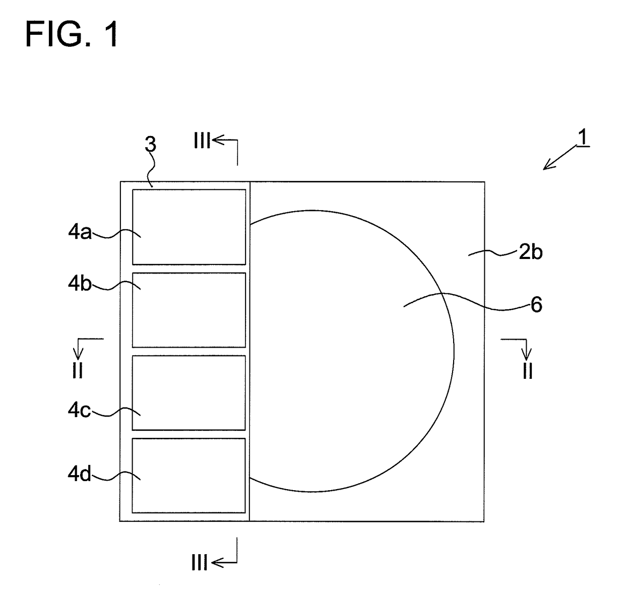
[0088]The device having electronic components mounted therein of the first exemplary embodiment was manufactured so that the top surface had the mode shown in FIG. 11 and the cross-section through the center had the mode shown in FIG. 2.

[0089]In this example, one BGA (Ball Grid Array) type package (external dimensions: 38 mm×38 mm; power consumption: 7W; number of input / output terminals: approximately 800 pins) on which an image processing processor chip was installed was used as the first electronic component. Also, four DDR-DRAM packages (external dimensions: 10 mm×10 mm; number of input / output pins: approximately 60 pins) were used as the second electronic components.

[0090]The spacer used in this example was made of glass epoxy resin (FR4) having thermal conductivity of approximately 0.36 W / mK. The shape of the spacer is an inverted groove shape as shown in FIG. 2, the shape of the flat surface is as shown in FIG. 4, with the shape being such that when the image processing proces...

example 2

[0101]A device having electronic components mounted therein of a second exemplary embodiment whose cross section near the center has a mode as shown in FIG. 19 was manufactured.

[0102]In this example, one image processing processor package that was the same as that of example 1 was used as the first electronic component. In addition to eight DRAM packages that were the same as those of example 1, sixteen chip capacitors (so-called 1005 type: 1.0 mm×0.5 mm) having a capacitance of 100 pF were used as the second electronic components. The DRAM packages were stacked two each as shown in FIG. 19, so the DRAM packages formed 4 sets. A flexible circuit board that was the same as that of example 1 was used as the flexible circuit board.

[0103]The spacer that was used in this example was glass epoxy resin (FR4) having a thermal conductivity of 0.36 W / mK, and was formed beforehand by a machining process such that it has a groove section for accommodating the second electronic components. In ad...


PUM

PropertyMeasurementUnit
temperatureaaaaaaaaaa
operating temperatureaaaaaaaaaa
temperatureaaaaaaaaaa

Abstract

A device having electronic components mounted therein has a first electronic component having an external terminal on a first surface and a heat spreader on a second surface, at least one second electronic component that is placed in the direction of a second surface of the first electronic component, a flexible circuit board that is electrically connected to the first electronic component and at least one second electronic component, and at least the part to which at least one second electronic component is connected is located on the second surface side of the first electronic component, and a spacer that is located between at least part of the flexible circuit board and the second surface of the first electronic component. The spacer can prevent heat from the first electronic component from being directly transferred to the second electronic component.

Description

CROSS REFERENCE TO RELATED APPLICATIONS[0001]This application is a National Stage of International Application No. PCT / JP2008 / 063007, filed Jul. 18, 2008, which claims priority from Japanese Patent Application No. 2007-188287, filed Jul. 19, 2007, the contents of all of which are incorporated herein by reference in their entirety.TECHNICAL FIELD[0002]The present invention relates to a device having electronic components mounted therein, and more particularly to a device having a plurality of electronic components that are mounted 3-dimensionally therein, and to the manufacturing method thereof.BACKGROUND ART[0003]As electronic devices become more compact and multi-functional, and from the necessity of high-density mounting of electronic components, 3-dimensional mounting technology for mounting electronic components such as semiconductor devices in the stacking direction is being developed.[0004]FIG. 21 shows a schematic cross-section view of a 3-dimensionally mounted semiconductor ...

Claims


Application Information

Patent Timeline
Patent Type & Authority Patents(United States)
IPC IPC(8): H05K7/20H01L25/065
CPCH01L25/0652H01L25/165H05K1/189H01L23/367H01L23/5387H01L23/642Y10T29/4913H05K2201/056H05K2201/2036H01L2224/16H01L2924/09701
Inventor YAMAZAKI, TAKAOWATANABE, SHINJIMURAKAMI, TOMOOFUJIMURA, YUUKIOSU, RYOJISUZUKI, KATSUHIKOMASUDA, SHIZUAKISATO, NOBUYUKIWADA, KIKUO
Owner NEC PLATFORMS LTD
Learn More